Introduction to pn junction Theory
a P-N Junction Is where two types of semiconductor materials, one with extra positive charges (p-type) and other with extra negative charge (N-type) meet. This junction creates special electrical behavior and forming the basis for Diodes and transistors in electronics.
In our previous tutorial we already discussed about fundamentals of diodes – Diode Definition, Types of Diodes in this tutorial, we lookout the P-N junction Theory of semiconductor.
Definition of P-N junction Theory
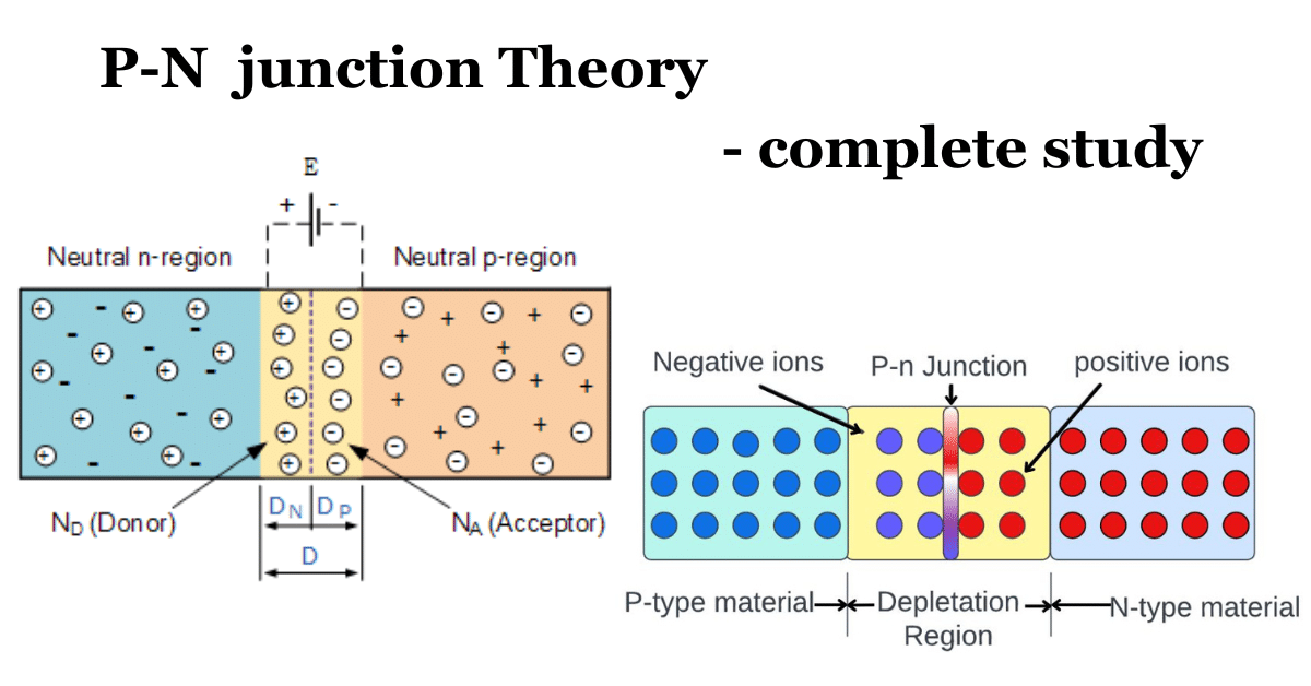
PN junction is where The P type and N type semiconductor materials meet in crystal. The “p” side has an excess of holes. And the “n” side has extra electrons.
This setup allows electric current to flow in only one direction. These junctions Are the foundation of electronics devices like diodes, transistors, LED, solar cells.
The PN Junction holds vital characteristics for contemporary semiconductor electronics. While both P-doped and N-doped Semiconductor exhibit conductivity, the junction between them can experience a depletion of charge carriers based on the relative voltages of the semiconductor region.
Through control of charge carrier movement across this depleted layer, p-n Junction are frequently employed as diodes. These diodes serve as electrical components permitting the passage of electricity in one direction while restrict in the opposite direction.
What is PN junction Theory
P type semiconductor: this type of semiconductor material has an excess of positively charged “holes” which are essentially locations where an electron can exist. These holes behave as positive charges.
N Type semiconductor: this semiconductor material that has an excess of negatively charged electrons.
when a P type semiconductor fused or brought into contact with an N type semiconductor a boundary formed between them creating the PN junction.
At this junction two significant phenomena occur.
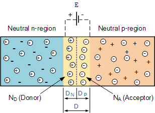
Diffusion: electronics from the N-type region diffusion into P-type region, and holes from the P-type region diffuse into the N-type region. This movement of charge continues until an equilibrium is reached. This diffusion of charge carriers across the junction creates a depletion region.
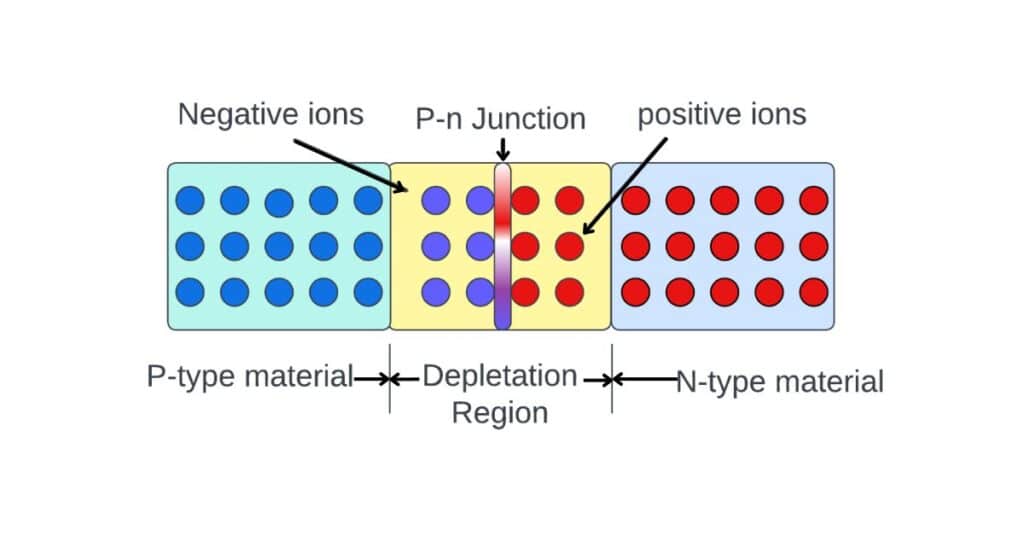
Depletion region: as electrons from the N-type region moves into the P-type region and vice versa, they leave behind charged ions. This accumulation of ions results in the creation of a depletion region near the junction, which lacks a free charge carrier. This depletion region acts as a barrier to further diffusion of charge carriers.
Formation of potential barrier: The potential barrier further movement of majority charges carriers across the junction leading to the establishment of an equilibrium state known as the “barrier potential” or “built-in potential”.
prevents the movement of charge carriers and creates an electric field across the junction. This field opposed further movement of charge carriers, formatting Potential barrier.
History of PN junction theory
The p-n junction, a basic component of contemporary electronic, has a long and intriguing history. here are some of its major achievements.
Early observation (before 1930s)
Rectifying metal-semiconductor connections: researchers discovered that some metal semiconductors contain permitted current to flow in just one direction, pointing to the possible of the p-n junction.
Cat’s whisker detectors:
These early radio detector rectified radio signals using a pointed metal contents on a semiconductor, and established the framework for p-n junction diodes.
The p-n junction was invented in the 1930s
Russell Ohl, an American scientist at bell labs, is credited with accidently finding these junctions while researching with silicon in 1939. When he linked an n-type wafer to a p-type silicon wafer, he saw a rectifying effect.
Ohl’s finding led to the construction of the first silicon rectifier in the 1940’s. signaling a dramatic department from metal rectifiers.
Theoretical comprehension (1940’s to 1950’s)
In 1947, another Bell Labs researcher, William Shockley, expanded on Ohl’s work and presented a detailed model of the p-n junction in his book.
Additional Development (1950’s to present)
The working of p-n junction serves as the heart of many semiconductor devices including diodes, transistors, integrated circuits and many more. Today This technology become a key component in modern electronics, enabling a wide range of applications from cellular phone to medical equipment’s.
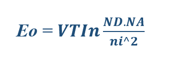
P-N junction formula
Were,
EO is the zero bias junction voltage
VT is the thermal voltage at room temperature
ND and NA are the impurity considerations
ni is the intrinsic concentration
What are the Composition use in PN junction
Silicon (Si):
silicon is the most widely used material for both (P and N) type because of its wealth, ease of processing and favorable electrical properties. It can dope with elements from Ⅲ (boron, aluminum) or group Ⅴ (phosphate, arsenic) to create p or n type semiconductor respectively.
Germanium (Ge):
a group ⅠⅤ elements like silicon, was also an early chose for both p and n type semiconductors. It has high cost and sensitivity to temperature that’s make him suitable for more applications.
Gallium arsenide (GaAs):
this used mostly in optoelectronic devices, such as light emitting diodes (LEDs) and lasers. It can dope with zinc (Zn) for creating p-type or Selenium (Se) to create n-type semiconductor.
Indium phosphide (InP):
Indium phosphide is an Ⅲ – ⅤⅠ compound semiconductor with optoelectrical applications. It can be doped with zinc (Zn) or magnesium (Mg) to create a p-type or Sulphur (S) or selenium (Se) to create an n-type semiconductor.
Silicon Germanium (SiGe):
SiGe is an alloy of silicon and germanium that combines the desirable property of both materials. It has high mobility that silicon and can be used for high-speed transistors.
Importance of PN junction theory in electronic
The p-n junction allows current to flow in one direction only is a very useful in creating many other devices. It will block current flow in opposite direction. so according this we have discussed the significance and applications in below
Applications
Diodes: used in rectification for converting AC To DC current
Solar cells: for generating electricity from sunlight by utilizing the photovoltaic effect.
Light Emitting Diodes (LED’s): that’s emits light when current passes through it it uses in displays, indicators etc
Integrated circuit: in IC’s PN Junctions uses to create complex electronic circuits.
Frequently asked questions
Q. What is use of pn junction diode?
Ans: Rectification, condenser, regulator, amplifier are the common uses of pn junction diodes also there are many several uses.
Q. What is breakdown voltage of pn junction diode?
Ans: a breakdown voltage in diode is when the reverse-bias voltage at which current increases suddenly across it. If the reverse bias voltage is increases then current through PN junction will also increases resulting breakdown voltage forms.
Q. How is depletion layer formed?
Ans: when the diffusion of holes and electronics in N and P type regions to neutralized the both regions of the p-n junction that make cause of Depletion region formation
Q. What is called tunnel diode?
Ans: a special type of diode which has effectively negative resistance due to its quantum mechanical effect that diode known as Tunnel diode.
Q. why we use tunnel diode?
Ans: the tunnel; diode provides very fast switching devices in computers. It can also use in High-frequency oscillators and amplifications.
Conclusion
The P-N junction theory in semiconductor explains how the combination of P and N type semiconductors creates a junction. This junction forms a depletion region that control the floe of current when a voltage is applied to it. Its’s fundamental to diodes and transistors, enabling essential functions like rectifications and amplifications in electronics.
Also read
Follow to the blog ETechSpark.com for more articles on electrical engineering, electronic and tech updates.
please leave your question in the comment section, give us your valuable feedback.