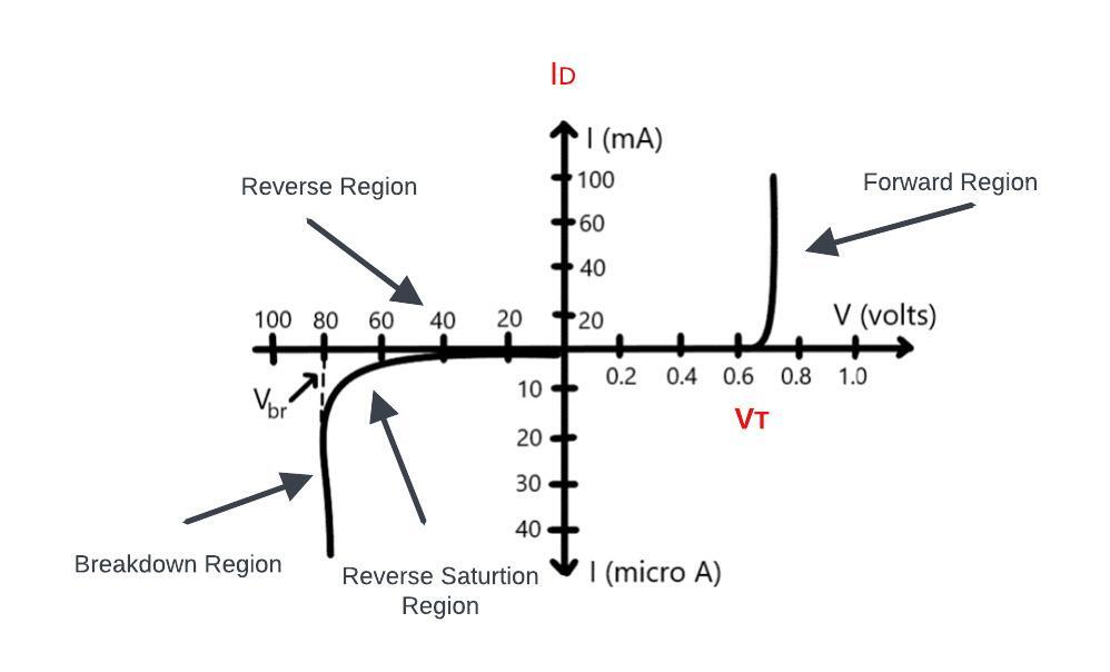
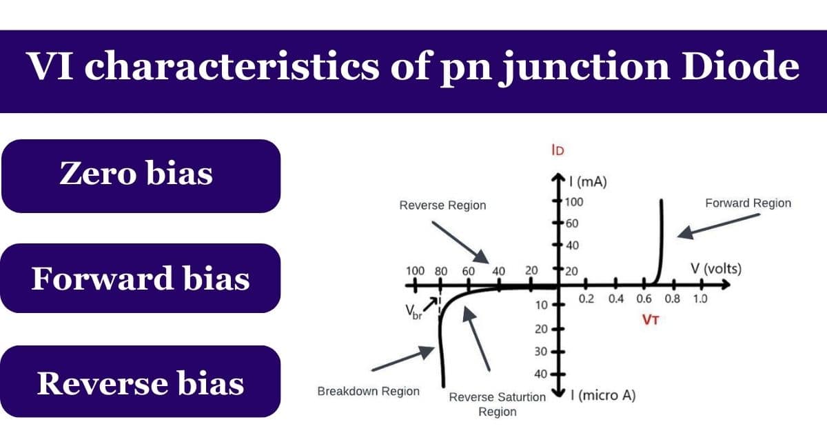
The VI characteristics of a pn junction diode describe the relationship between the voltage applied across the diode (V) and the resulting current flowing through the diode that is (I).
After discussing the pn junction theory let us see what are the VI characterises of pn junction diode.
the relationship is typically represented graphically, showing how the diodes behaves under different Forward and reverse bias conditions.

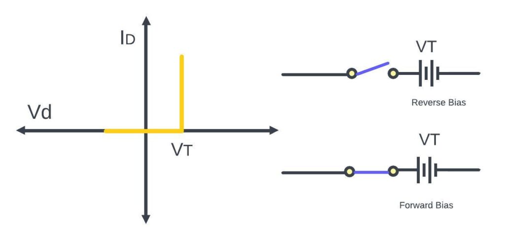
In a forward bias, the diode conducts with low resistance, allowing a significant current flow.
In reverse bias, the high resistance and only a small leakage current passes through until certain reverse voltage threshold, after which it might experience breakdown and allow a substantial reverse current.
The VI characterises curve helps to understanding the diodes behavior and its applications in electronic circuits.

VI characteristics curve pn junction Diode

The V-I characteristics of the PN junction can be explained in three cases:
- Zero bias or unbiased
- Forward bias
- Reverse bias
Zero Bias/ unbiased:
In Zero Bias conditions there is no any external influence that means no any external voltage applied across the diode. A tiny or minimum current is flow is also called as leakage current flow due to the diode’s natural properties. In unbiased diode not conducting so much it like a calm lake without much movement.
Forward Bias:
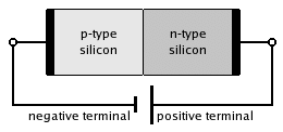
forward bias refers to the conditions in which positive voltage is applied to the p-type semiconductor material and a negative voltage to the N-type material in a PN junction diode.
This applied voltage reduces the potential barrier at the junction, allowing majority charges carriers (holes in the p-type and electrons in the N-type) to move across the junction more easily. (typically, around 0.6 to 0.7 volts for silicon diode)
It results in an increased flow of current through the diode. During forward bias, the diode in its conducting state and exhibits a significant flow of current with a exponential relationship between the applied voltage and the resulting current, as described by the diode equations.
As more voltage in the right way means way more current through the diode, thanks to the Shockley diode equations.

Where;
- I is the diode current
- I0 is the reverse saturation current
- e is the electron charge
- v is the applied voltage
- n is the ideality factor
- k is the Boltzmann constant
- T is the absolute temperature
in forward bias the external voltage is applied in the right direction. It will increase current so lots of electrons start flowing through, creating a strong current and a small voltage drop occur across the diode, letting the current move smoothly, like a river flowing downstream.
Reverse Bias:
A reverse bias occurs when a PN junction diode is subjected to a negative voltage at the P-type material (anode) and a positive voltage at the N-type material(cathode).
In these conditions, the externally applied voltage increases the potential barrier at the junction, widening the depletion region and reducing the flow of majority carriers (holes in the p-type and electrons in the n-type) across the junction.

Consequently, only a small leakage current, typically in the nanoampere range, flows through the diode.
At a certain voltage, known as the breakdown voltage, the diode experiences a sudden increase in current due to a phenomenal called the avalanched effect or Zener breakdown, depending on the diode types.
a Reverse bias, is like in Zener diodes, that helps to controlling voltage and protect circuits by maintaining the diode in a specific state that ensures stability and safeguards against power surges.
Knee voltage:
The threshold voltage in the forward bias region where the diode starts conducting is often referred to as the “knee voltage”. It’s the point where the diode begins to allow significant current flow.
Exponential relationship: the VI curve follows an exponential relationship forward bias, the current increases exponentially with voltage due to the exponential relationship between current and voltage in the diode equation.
These VI characteristics of a pn junction diode are crucial in understanding the behavior of diode in various circuits and applications, enabling their effective use in rectification, signal modulation, and other electronic applications.
Also Read :
- How Freewheeling Diode Work: Easy Explanation
- What is P-N junction Theory of semiconductor
- Diode Definition, Types of Diodes, V-I Characteristics & Application
Conclusion:
The vital VI characterises of a PN junction diode includes its behavior in forward and reverse bias, an exponential voltage- current relationship, a forward voltage drop, a cut-in voltage and traits like junction capacitance and reverse recovery time. These define its role in electronic for tasks such as rectification and signal modulation.
Follow to the blog ETechSpark.com for more articles on electrical engineering, electronic and tech updates.
please leave your question in the comment section, give us your valuable feedback.
