Schottky diode definition
A Schottky diode is a semiconductor device formed by the junction of a metal and a semiconductor material if we see typically Schottky diodes are made of silicon or gallium arsenide.
Unlike the regular diode these diodes are have a low Forward voltage drop around 0.2 to 0.3 volts. Due to fast switching characterises this make them useful in high-frequency and high-speed applications
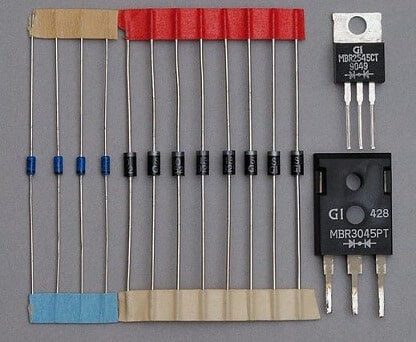
Schottky diodes are named after the German physicist Walter H. Schottky.
Among the various kinds of diodes – such as LED’s, Zener diodes, photodiodes, Schottky Diode, avalanched diodes, PN junction diodes and others
let us zoom in on the Schottky diode for this article.
What is a Schottky diode?
The metal-semiconductor junction in a Schottky diode can be formed using various metals and semiconductors materials. That commonly used various metals like as titanium, platinum, chromium, or tungsten.
The choice of metal depends on various factors such as thermal stability, compatibility with martial also descried electrical properties.
If we apply high frequency as a input signal for diode then a normal diode gives Bad signal at output while this diodes gives a clear and good distortion less output signal at output. That is why Schottky diodes are used in high frequency applications like as- RF Mixer and detectors, signal clipper and clampers etc.
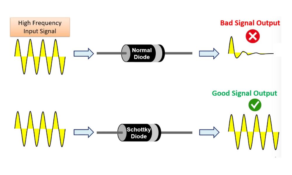
A Normal diode cannot respond to the reversal of the applied voltage at very high frequencies. But a Schottky diode perform a better role.
Schottky Diode Construction
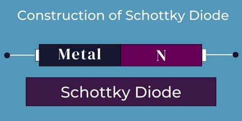
As we already discuss working of diodes in our previous posts, so now discuss construction and working principle of Schottky diode step by step
Working principle of a Schottky diode
Firstly, understand the Schottky diodes are operates on the metal-semiconductor junction principle, so here is the simplest explanation of how a Schottky diodes are works.
Metal-semiconductor (M-S) junction
The crucial parts of this diode are the metal-semiconductor junction. These metal layers are formed like as platinum or tungsten etc.
In a regular p-n junction diode configuration semiconductor materials are in both sides of the junction but in Schottky diode both sides are different one side made up of metal and other one is from semiconductor as we can see in above diagram.
What is a Schottky barrier?
Hence the contact is happening between the metal and semiconductor that results in the creation of a barrier at the junction and this barrier is a potential energy barrier because it caused by the difference in electron work functions between metal and semiconductors.
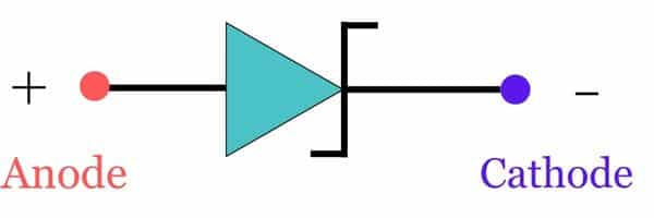
Schottky Diode Symbol
V-I characteristic of Schottky diode
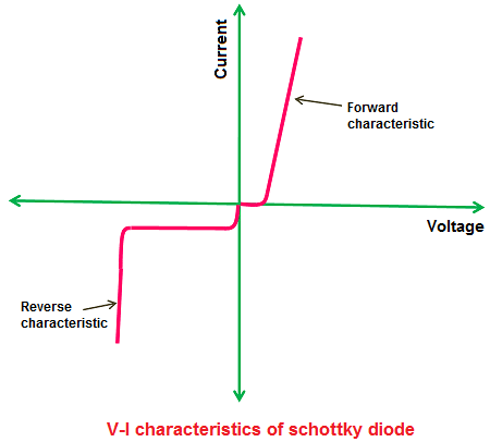
Characterises of Schottky diode
Unbiased bias
An unbiased refers to a Schottky barrier diode in a state where no external voltage is applied across its metal-semiconductor junction so there is no any electron flow this term also known as Zero bias of diode.
Forward bias
When a forward voltage is applied across the diode (positive voltage at anode and negative at cathode that is at semiconductor side) then the potential barrier is lowest and it causes current to flow in forward direction.
Electrons from the metal with higher energy can now easily move into the semiconductor material creating electrons to flow. If the applied voltage is greater than 0.2 volts then forward bias happen.
Reverse bias
In a reverse-bias when a reverse voltage is applied (negative on the metal side and positive on the semiconductor side) then the diode quickly transitions from a low to high resistance state.
This rapid changes in resistance is known as the “snap-off” effect and this effect is occur due to the absence of a depletion region in this diode.
The reverse-biased is characterises by its fast response to changes in voltage polarity.

Energy band diagram of Schottky diode
The energy band diagram of n-type semiconductor with metal is shown as below figure. Here te work function of a metal is greater than the work of semiconductor.
The metal side has a continuous energy band corresponding to the metal’s fermi level. The fermi level in metals is relatively high that indicated a large number of available electrons.
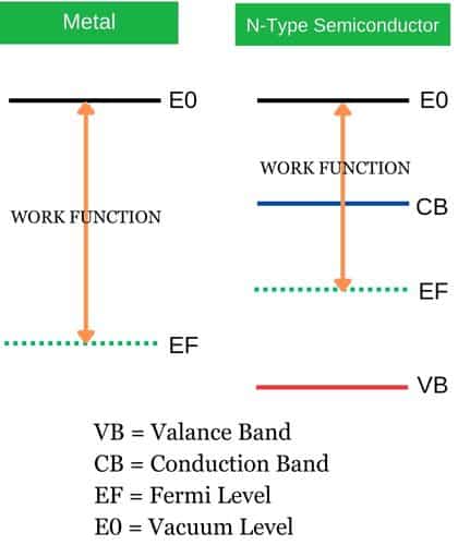
We understand that electrons at high energy levels possess greater potential energy compared to electrons at lower energy levels.
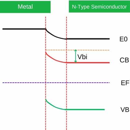
The energy band diagram presented below illustrates the configuration of energy in both metal and n-type semiconductor after their contact.
Schottky Clamped Transistor
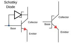
Schottky Clamped Transistor integration is an integration of Schottky diode with a Bipolar junction transistor (BJT). It has developed for enhancing switching speed reducing the base current also that prevents the transistor from saturation by diverting the excessive input current.
- Schottky-Clamped TTL:
In a some TTL (Transistor-Transistor Logic) circuits especially for high-speed circuits these diodes are used to clamp the voltage across the base-emitter junction of transistors.
This will help to reduce the switching time and improving overall speed performance of the TTL circuits.
- Schottky-clamped ECL:
A ECL (Emitter-Coupled Logic) circuit known as for their high-speed operation. It often use this diode to clamps the transistor’s base-emitter junction voltage.
This helps to minimize the switching time of the transistors and boost the overall speed performance of ECL Circuits.
Relationship between temperature and loss on SBD
The relationship between temperature and loss on Schottky Barrier Diodes is primarily characterized by the increases in reverse leakage current with elevated temperature.
As the temperature rises the intrinsic carrier in the semiconductor material gain energy that’s leading to a higher probability of thermally generated electrons-hole pairs.
The rising in temperature also causing changes in the diode’s electrical characterises. Therefore, it is very crucial to consider temperature effect when circuit is design.
Types of diodes
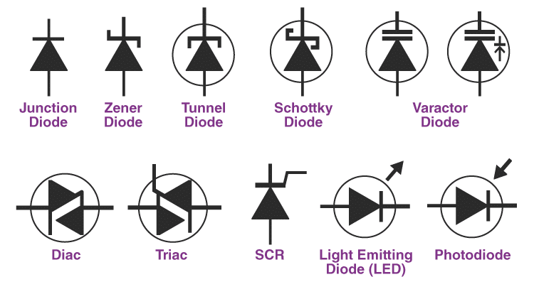
we have already a brief tutorial on “Types of diodes ” so you can check this one for more information.
Difference between Schottky and P-N junction Diode
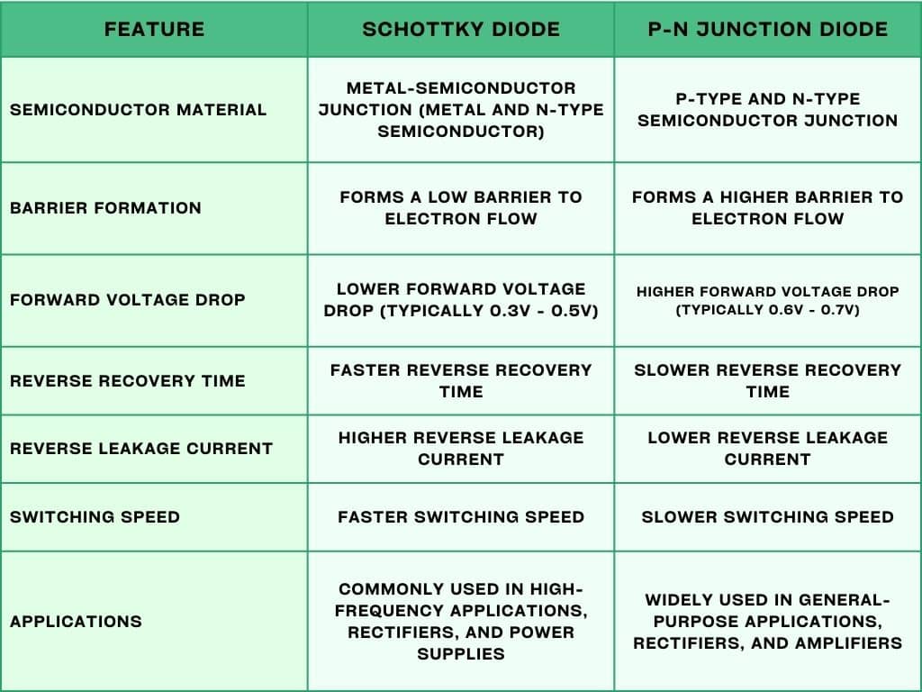
What is a Schottky diode used for
applications of Schottky diode are various in electronic and electrical circuit designs such as follows-
Rectification: they can efficiently convert alternative current to direct current in power supply circuits.
Switching: a Schottky diodes has fast switching characterises that makes them suitable for high-frequency circuits and also applicable for signal demodulator.
Voltage Clamping: for protecting sensitive components by limiting voltage spikes in circuits.
RF Circuits: applications of Schottky Diodes are in radio frequency for mixing and detection.
Solar Cells: for preventing reverse current flow in photoelectric (Solar) Cells to optimize energy conservation.
High speed Data Transmission: in communication system these diode plays a major role in high-speed data transmission, acting as fast-switching components in signal processing and modulation / demodulation circuits.
Advantages
- Low junction capacitance
- Fast reverse recovery time
- High current density
- Low forward voltage drops or low turn on voltage
- High efficiency
- Schottky diodes operate at high frequencies.
- Schottky diode produces less unwanted noise than P-N junction diode.
Disadvantages
- Large reverse saturation current
- Lower Reverse Breakdown Voltage
- Temperature Sensitivity
FAQs
Q. Schottky diode vs. Zener diode
Ans:
| Parameter | Schottky diode | Zener diode |
|---|---|---|
| Junction Type | Metal-semiconductor junction | P-N junction |
| Barrier Type | Low forward voltage drops (typically 0.3V – 0.5V) | Higher forward voltage drops (depends on Zener voltage) |
| Reverse Breakdown | Does not rely on reverse breakdown; low reverse voltage tolerance | Designed for specific reverse breakdown voltage (Zener voltage) |
| Voltage Regulation | Not designed for voltage regulation | Specifically designed for voltage regulation |
| Applications | Commonly used in rectifiers, power supplies, high-frequency applications | Used for voltage regulation, voltage reference, and protection circuits |
| Reverse Leakage Current | Higher reverse leakage current | Lower reverse leakage current |
| Switching Speed | Faster switching speed | Slower switching speed |
Q. Why is Schottky are faster diodes?
Ans: Schottky diode are faster because they have a lower forward voltage drop use a metal-semiconductor junction so they enabling quicker switching between on and off states.
Q. Is Schottky bidirectional diode?
Ans: No, this diode is not unidirectional so it allows current in only one direction that is anode to cathode that is from metal to semiconductor side and block current in opposite direction.
Q. Who invented Schottky diode?
Ans: the Schottky diode is named after physicist Walter Schottky who invented it in 1938.
Also read:
Zener Diode – Working, Characteristics and applications
How Freewheeling Diode Work: Easy Explanation
What is P-N junction Theory of semiconductor
Diode Definition, Types of Diodes, V-I Characteristics & Application
Schottky Diode Summary
Schottky Diodes are a semiconductor device with a metal-semiconductor junction. They have a low forward voltage drop also provides fast switching speed with a minimal reverse recovery time
These diodes are commonly used in power supplied and high-frequency circuits also hey offer efficiency advantage but have limitations in reverse voltage handling.
