What is a Common Drain MOSFET Amplifier
A common Drain MOSFET amplifier is an electronic setup that uses a specific type of transistors to boost the incoming signals. This amplifier is also known as a source follower amplifier.
A C.D. MOSFET amplifier is one of the basic three MOSFET configurations design which are
- common gate Mosfet amplifier (CG)
- common source Mosfet amplifier (CS)
these classes we have already discussed in previous tutorial, in this tutorial we will discuss all about the Common Gate MOSFET Amplifier- it’s operations, characterises – applications and all essential information’s.
Definition of Common Drain MOSFET amplifier
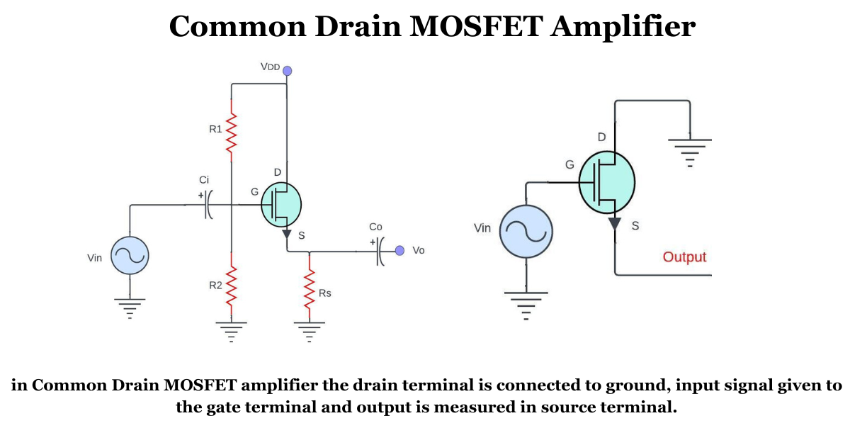
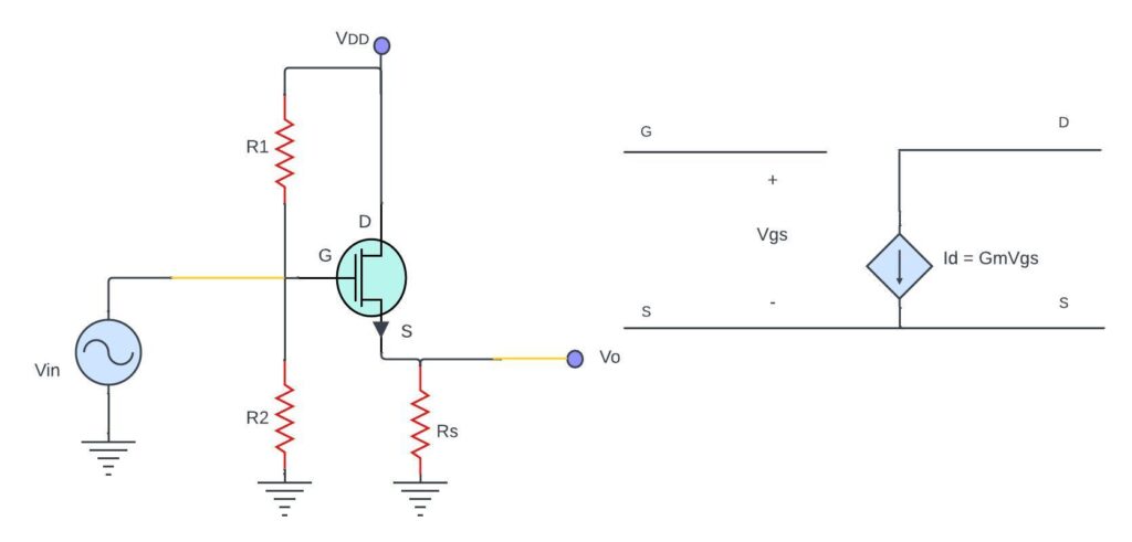
A Common Drain MOSFET amplifier where the drain terminal is connected to ground, the applied input signal is given to the gate terminal and output is measured in between source and ground terminal.
working principle of Common Drain MOSFET amplifier
in the previous tutorial we have already seen the common source and the Common gate MOSFET amplifiers configurations of so in this tutorial let us discuss the common drain MOSFET amplifier configuration of the and this configuration is also known as the source follower.
in this source follower configuration drain terminal is connected to ground, the input signal is applied to the gate terminal and output is measured in between source and ground terminal.
Note: in source follower the output and the input signal will be in the same phase.
Common Drain MOSFET amplifier circuit Diagram
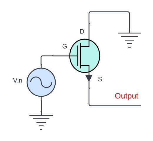
the drain terminal is common between the input and the output side and hence it is known as the common drain amplifier configuration
Operation of Common Drain MOSFET amplifier
small-signal analysis of C.D amplifier
output impedance voltage gain so for this circuit now let us find the input impedance the output impedance and the voltage gain here this fixed gate voltage
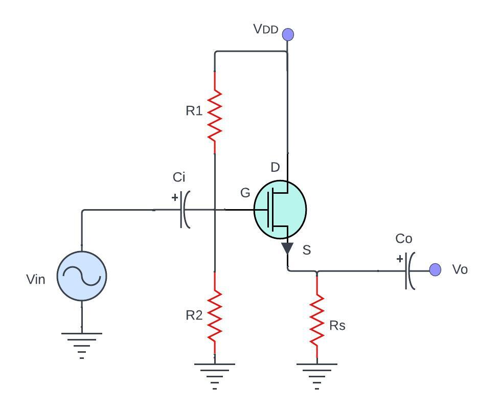
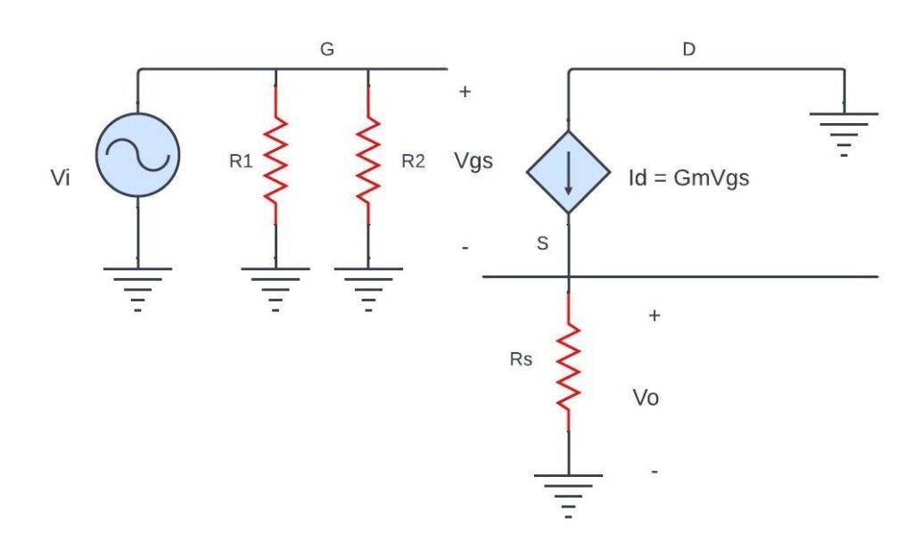
now if we talk about the small signal Ac analysis then the capacitors (Co) will act as a short circuit and the dc voltage source vdd will act as a zero
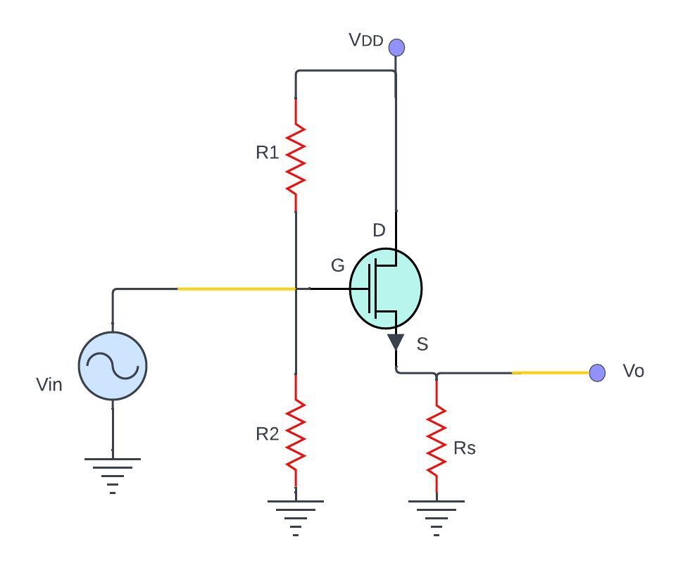
and then after we need to replace the Mosfet by the small signal model
so here input is given between the gate and the ground terminal and since the drain terminal is at ac ground so these two resistors r1 and r2 will appear between the gate and the ground terminal and here this source resistor is appearing between the source and the ground terminal so if you see the small signal equivalent circuit then it will look like this
input impedance
let’s find the input impedance
the input impedance is the ratio of this input voltage to the input current and in this case since the gate acts as open circuit at the low frequencies
VIN / In
Vin = Iin (R1 || R2)
Vin / In = Zin = R1 || R2
the input impedance of this mosfet is ideally infinite but because of this resistor r1 and r2 the input resistance will be finite
for large input impedance
the value of resistor r1 and r2 should be as high as possible and typically the value of this r1 and r2 is in mega ohms
voltage gain
now here the voltage at G node is equal to Vin so if we apply the kvl in this loop then we can write
Vin – Vgs – Vo = 0
Vgs = Vin – V0
now let us apply the kcl at S node
Vo / Rs = gm * Vgs
V0 / Rs = gm * (Vin – V0)
V0 / Rs + gmV0 = gmVin
V0 / Vin = gmRs / 1 + gmRs
Now Here
the voltage gain that is Vout / Vin will be always less than 1 and if this gmRs is much greater than 1 then the voltage gain is approximately equal to 1
Expression of the voltage gain including the effect of the output resistance
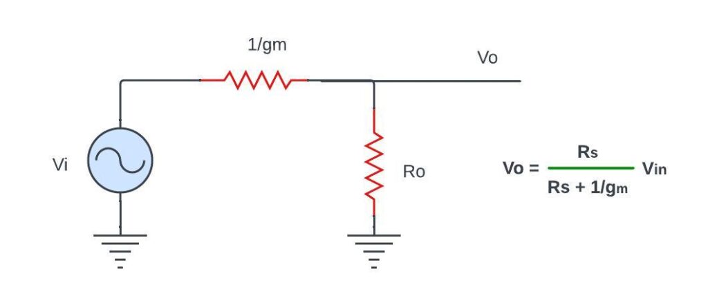
Av = Rs || r0 / 1/gm + (Rs || r0)
If the output resistance of this Mosfet is infinite
Av = Rs / 1 / gm + Rs
now from this expression if we draw the equivalent circuit then it can be drawn like this
output impedance
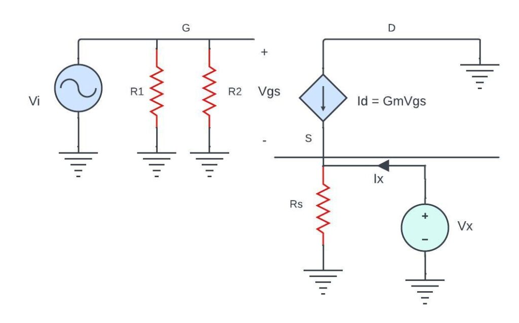
For finding the output impedance firstly apply the test voltage and lets find a test current for that we have to make all independence sources in the circuits as zero.
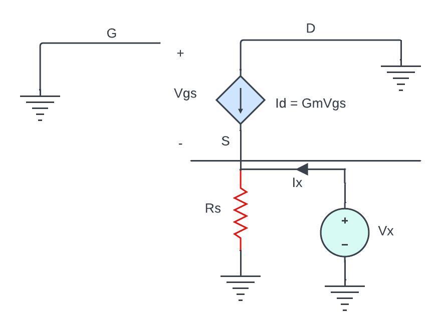
In the equivalent circuit
Vgs = -Vx
now, applying kcl at node x
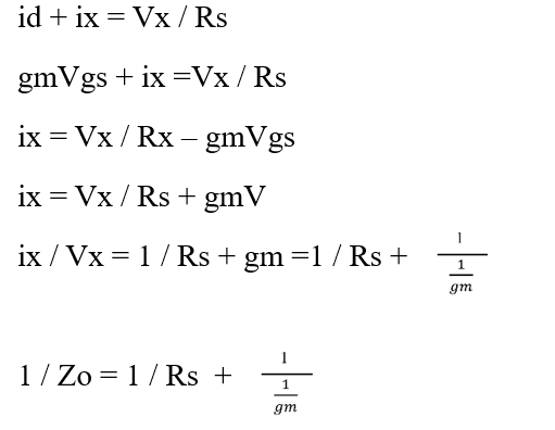
Zo = Rs || (1 / gm)
With finite output resistance of Mosfet the output impedance
Zo = Rs || ro || (1/gm)
The output impedance of source follower is low typically tens of ohms
this low output impedance of the source follower is particularly useful in driving the low impedance load
Characterises of Common Drain MOSFET amplifier
Voltage gain: the common Drain MOSFET amplifier, also known as source follower offers a voltage gain less than unity. While it does not amplify voltages significantly, these amplifiers provide excellent current gain. That is make them suitable for impedance matching between different circuits stages.
High input impedance: these amplifiers have high input impedance. That is characterises make him suitable for easy to interface with preceding stages without causing a substantial load on the driving circuits.
Low output impedance: the output impedance of these amplifier is low. Because of that it can drive load effectively and maintain signal integrity across the connected components.
Stability and linearity: by maintaining Stability and linearity design an amplifier circuit is a very crucial aspect. The common drain amplifiers offer good stability and linearity performance within its operating range. That is makes them suitable for signal processing.
Thermal stability: a C.D amplifier give good thermal stability, that’s ensure consistent performance even under varying temperature conditions. Heat dissipation and thermal stability are critical and important for amplifiers reliability.
Example
Q. for given figure determine the gain and input impedance
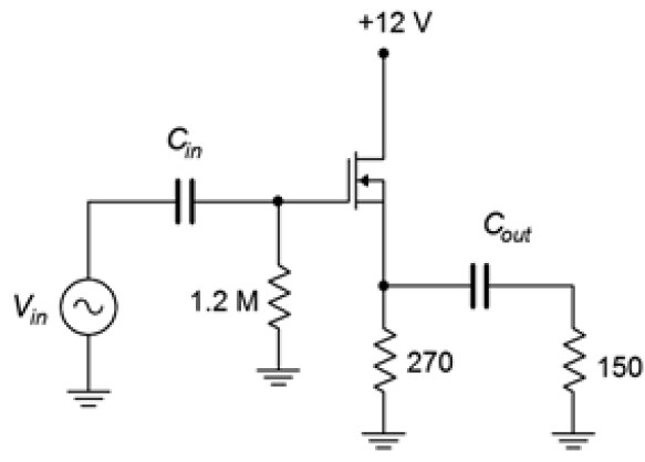
Assume Vgs(off) = -V and Idss = 30 mA
Solution: this amplifier has self-bias so firstly we need to determine gmoRS
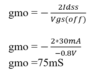
the dc source resistance is the 270 Ω biasing resistor resulting in gmo RS = 16.2 from the bias equation or graph this produces a drain current of 2.61mA
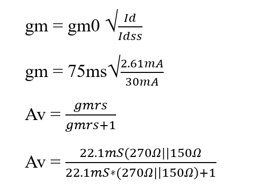
Av = 0.68
The input impedance is
Zin = 1.2MΩ || Zin(gate) ≈ 1.2M Ω
Advantages of Common Drain MOSFET amplifier
- High input impedance
- Low output impedance
- Excellent voltage following capability
- Thermal efficiency
- Wide bandwidth and frequency response
- Simple and varsities designs
- They have voltage buffering for ensuring stability
- Good at noise performance
Disadvantages of a Common Drain MOSFET amplifier
- Limited voltage gain
- Low power gain
- reduce signal swing
- voltage offset
- complex biasing requirements
- limited driving capability
Applications of Common Drain MOSFET amplifier
Audio Amplifications:
used in audio circuits such as in preamplifiers or headphone amplifiers, due to its ability to maintain signal integrity and low distortion.
Buffer circuits:
as an efficient voltage buffer between different stages of a circuit, that’s preventing signal degradation and keep maintaining stability.
Sensor interfacing:
used in sensor signal conditioning circuits, especially where the high input impedance is needed to avoid loading the sensor.
RF applications:
a Common Drain MOSFET amplifier is suitable for radio frequency applications where it can be utilized in RF power amplifiers or low-noise amplifiers due to its high input impedance and good frequency response.
Signal isolation:
this amplifier can be applied for signal isolation between different sections of a circuits to prevents interferences.
Medical electronics:
they can be found in various medical devices and instruments due to it’s reliability, stability and low distortion characterises.
Frequency Asked Questions
Q. Why is common drain used as buffer?
Ans: the drain terminal is common between the input and output, as an efficient voltage buffer between different stages of a circuit, that’s preventing signal degradation and keep maintaining stability that’s why common drain is used as buffer.
Q. Which amplifier is mostly used?
Ans: The common emitter circuits configurations are used mostly for various applications.
Q. Which amplifier has highest efficiency?
Ans: the class C amplifier offers high efficiency compared with other classes.
Q Which amplifier is best transistor or MOSFET?
Ans: the choice between transistor and MOSFET amplifiers is depends on the applications in voltages, currents, and impedances also for any special requirements. Transistors has high currents applications and MOSFETs are has high impedance and low power needed.
Also Read –
Common Source MOSFET amplifier
Types of MOSFET amplifiers – A comprehensive guide
Summery
The Common Drain MOSFET amplifiers, also known as a source follower offers high input impedance and low output impedance and near unity voltage gain. It is ideal for buffering and signal isolations between circuits stages.
Follow to the blog ETechSpark.com for understanding core basic and fundamental knowledge of electronic and electrical engineering and tech updates.
