What is a Common Gate MOSFET Amplifier?
A CG MOSFET amplifier is one of the basic three configurations design which are common drain (CD) and as we earlier discussed common source (CS) Mosfet amplifier In our previous tutorial in this tutorial we will discuss all about the Common source MOSFET Amplifier– it’s operations, characterises – applications and all essential information’s.
Definition of Common Gate Mosfet amplifier
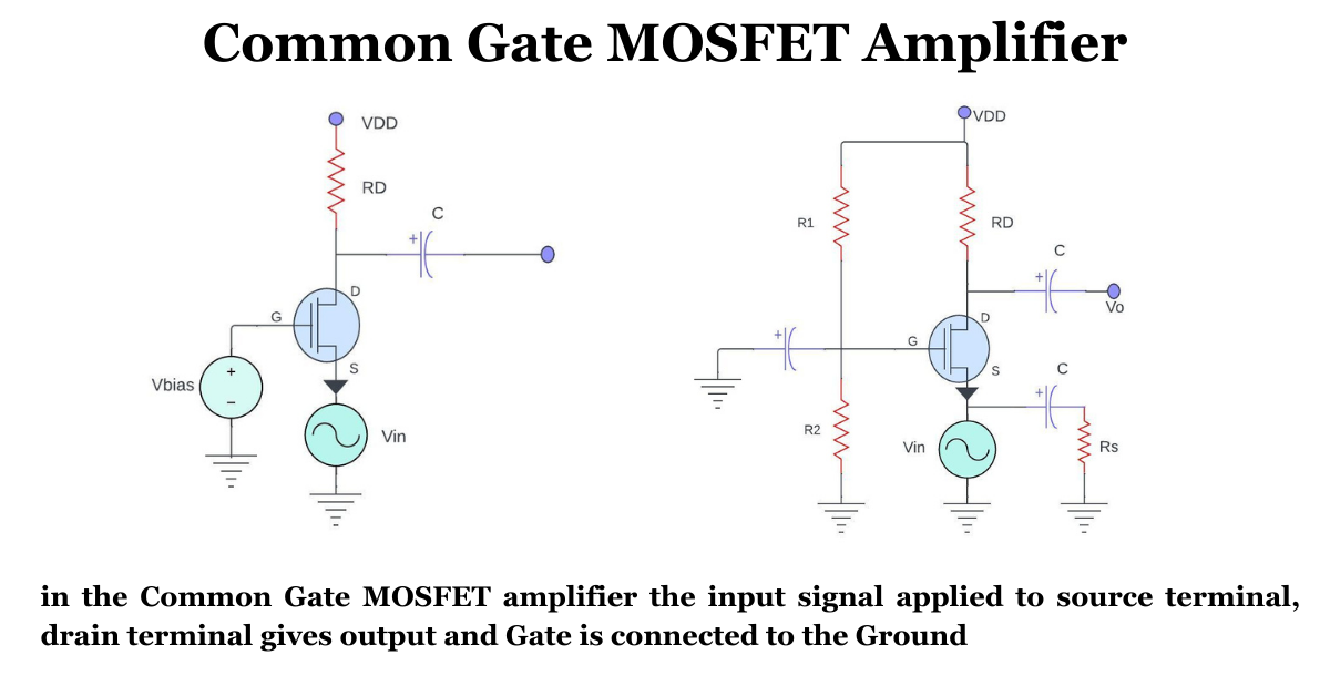
A Common Gate MOSFET amplifier is an electronic amplifier where the input signal is applied to the source terminal, drain terminal provides output and Gate is connected to the Ground terminal.
Working Principle of Common Gate MOSFET amplifier
The common gate MOSFET amplifiers a key circuit in electronic amplifier systems, it operates by utilizing the MOSFET source as an input terminal and the Drain as the output and gate is connected to the ground terminal. This configuration allows the input signal to control the transistors conductivity, modulations the current flow between source and drain terminal. Unlike the common source configuration, the common gate setup offers a high input impedance and low output impedance., making it suitable for high- frequency applications it has ability to maintain the precision signal processing and impedance matching.
Operation of Common Gate MOSFET amplifier
in case of the Common Gate Mosfet Amplifier, typically the gate terminal is at AC ground. So, the input is applied between the source and the ground terminal, while the output is measured between the drain and the ground terminal.
And since the gate terminal is at AC ground, hence the input is applied between the source and gate terminal while the output is measured between the drain and gate terminals. here the gate terminal is common between the input and the output side. therefore this configuration is known as the common gate amplifier configuration.
Common Gate MOSFET amplifier circuit Diagram
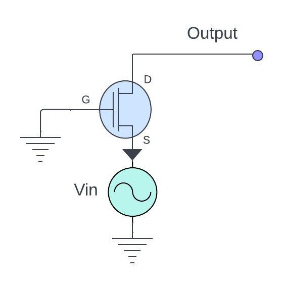
in this configuration, the input impedance of the amplifier is low. normally the input impedance of the amplifier should be as high as possible right, but in that case, the maximum applied input signal will appear across the input of the amplifier.
Because of that in some high-frequency applications, the Common Gate Amplifier is very useful. in such applications like as – the output of the antenna or the transmission line is given to the amplifier for the amplification. Or when the input impedance of the amplifier should match with the characteristic impedance of the antenna. And the impedance of the antenna or the transmission line is typically in the ohms. And in such cases, the common gate amplifier is suitable for impedance matching.
So, through a small signal analysis, we will find the expression of the input and the output impedance, as well as the voltage gain for this common gate amplifier.
small-signal analysis of common gate mosfet amplifier
firstly, we will find the expressions without voltage divider and without coupling capacitors this is a very basic circuit of the common gate amplifier along with the biasing. And here is the fixed voltage biased to the gate.
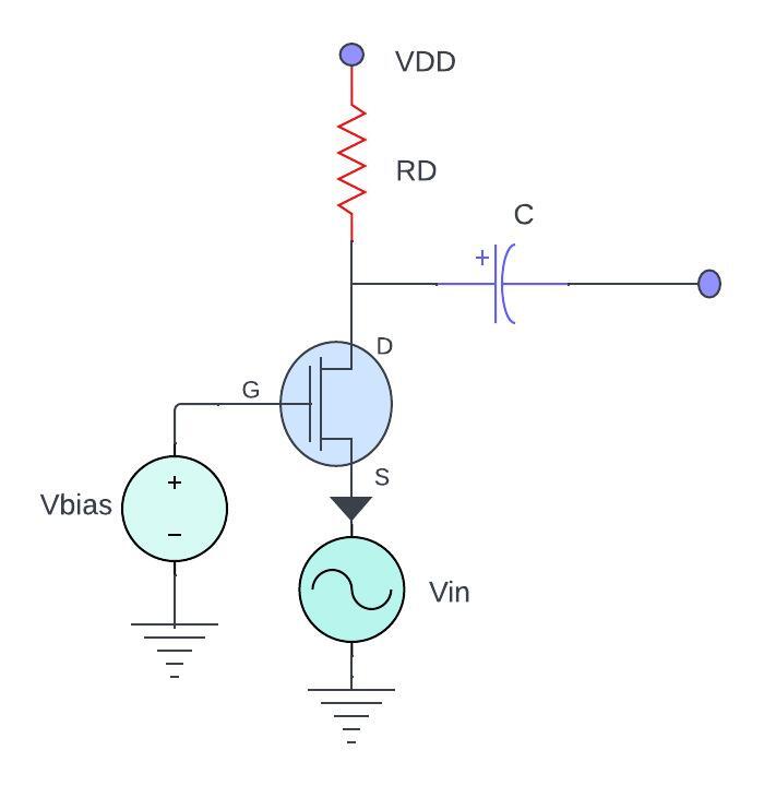
For AC small signal analysis, the AC input signal is applied at the source terminal. While the output is measured at the drain terminal. And for DC analysis, ac input signal will become as a zero. this is a biasing circuit for the common gate amplifier. Now, this biasing voltage and this drain resistor should be such that, the MOSFET operates in the saturation region.
Alright, so if we talk about the small-signal analysis, then for the AC analysis, this biasing voltage will act as a zero. And, this capacitor will act as a short circuit.
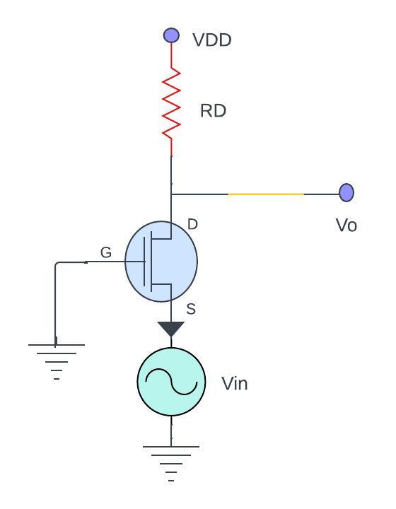
However, the drain voltage Vdd will also act as a zero. And then after, we have to replace the MOSFET by the small-signal model.
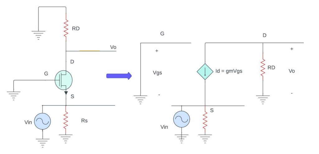
For the small-signal analysis, if we see, the input is appearing between the source and the ground terminal. And here this gate terminal is grounded.
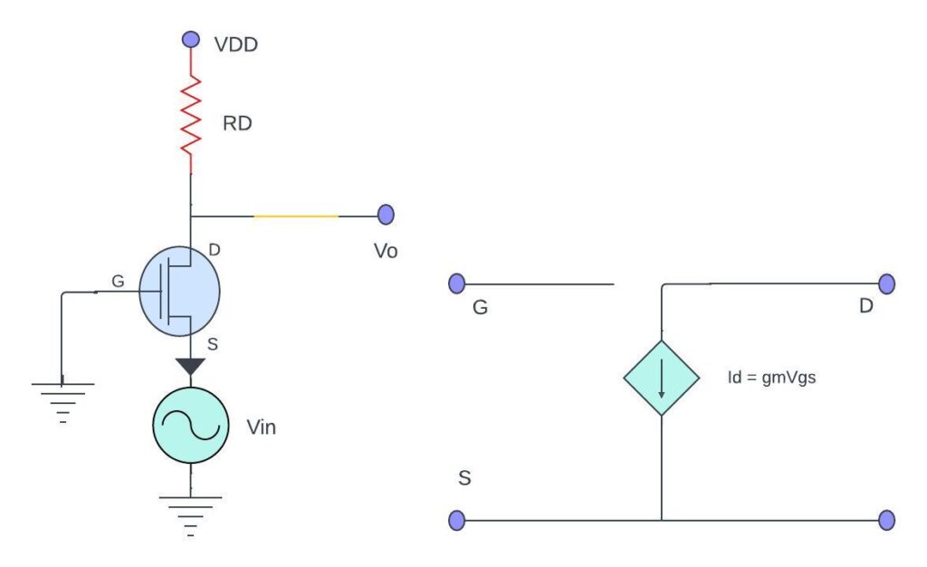
Also, the drain resistor Rd is appearing between the drain and the ground terminal. And as we know the small-signal equivalent circuit, then it will look like this.
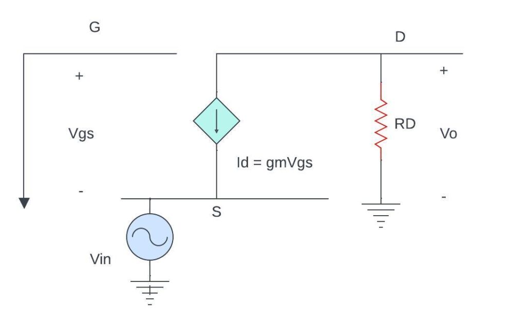
So, for this very basic common gate amplifier,
let us find the input impedance, the output impedance, and the voltage gain.
input impedance
if Vin is the input signal and Iin is the input current, then the ratio of this input signal to the input current will give us the input impedance. So, if we apply the KCL, at D node, then we can say that
Vin / Iin = 2In
I in + Id = 0
Iin = -Id = -gmVgs
Now, here the input is appearing between the source and the gate terminal. Or we can write is as the
voltage Vgs= -Vi
from this, the input current Iin which was -gm*Vgs can also be given as gm*Vin.
Vgs = -Vi
Iin = -gmVgs = gmVin
Vin / Iin = Zin = 1 / gm
output impedance
now let’s find the output impedance. the output impedance is Thevenin’s equivalent impedance which is seen from the output side by considering all the independent sources in the circuit as zero.
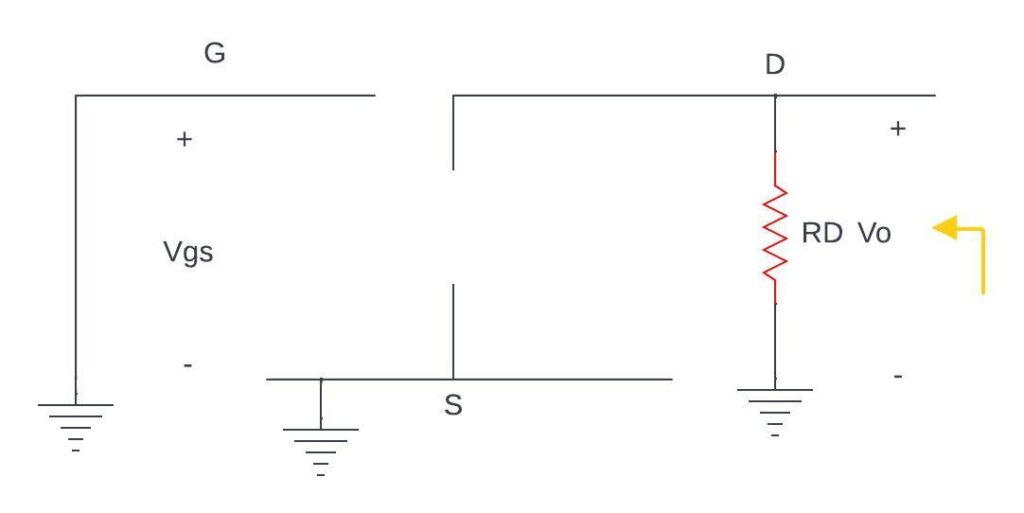
while finding this output impedance, we will consider this input signal as zero. now if we see, the gate and the source terminal, both are at the same potential.
Vgs = 0
Z0 = Rd
voltage gain
To find the voltage gain, firstly apply the KCL at D node. So, the current through this resistor
Rd = Io = Id
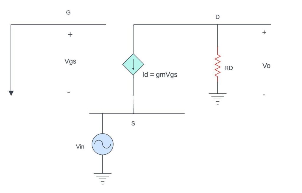
That means after applying the KCL we can write,
Io + Id = 0.
And here this output current is equal to Vo / Rd.
That means
Vo / Rd = -id = gm*Vgs
Now, as we have just seen, this Vgs = -Vi
That means we can say that
Vo / Rd = -gm*(-Vi)
Or
Vo/Vi = gm*Rd
that is the voltage gain of this common gate amplifier.
if we observe this expression, then we can say that the voltage gain of the common gate amplifier is like similar to the common source amplifier. But here, there is no negative sign. Meaning that, in this common gate MOSFET amplifier, the input and the output signal will be in the same phase.
Voltage divider circuit and coupling capacitor in common gate Mosfet amplifier
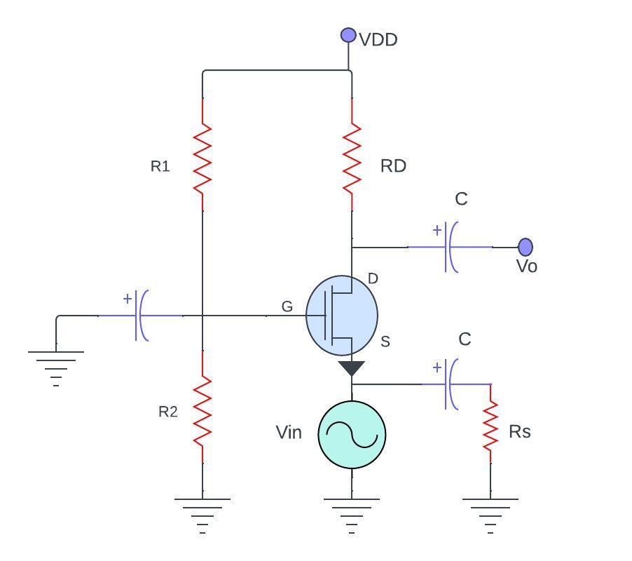
let us see, what is the impact of this source resistor on these above three parameters. for the AC analysis, all the capacitors will act as a short circuit at the operating frequency. And this DC voltage source will also act as a zero. After that, if we replace the MOSFET by the small-signal model, then the equivalent circuit will look like this
input impedance
let us apply the KCL at S node by applying the KCL, we can get the same result.
as we have seen, the input impedance is the ratio of the input signal to the input current. So, here this will be the input current. And the current through this source resistor
IRs = Vin / Rs
By applying the KCL at S node, we can write
IRs + Id = Vin/Rs
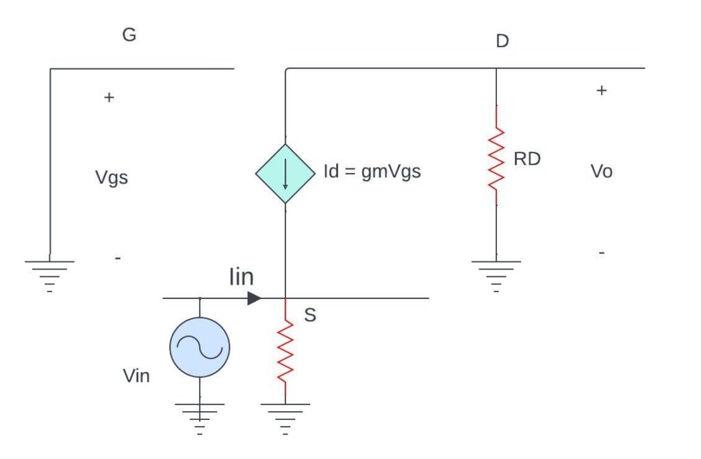
And the drain current Id = gm*Vgs.
And as we have seen, this Vgs = -Vin.
That means Iin + gm*Vgs = Vin / Rs.
Or if we further simplify input current Iin = Vin / Rs + gm*Vin Because here this vgs = -Vin. So, if we further simplify it then we can say that this input current is equal to Vin * [ gm +1/Rs]
That means Iin / Vin = 1/Zin = gm + (1/Rs)
Or we can say that Iin / Vin 1/Rs + (1/ (1/gm)) That means this input impedance is the parallel combination of 1/gm and Rs.
This is the input impedance of the amplifier.
output impedance
As we have seen, the output impedance is the Thevenin’s equivalent impedance which is seen from the output side, by considering all the independent sources in the circuit as zero. To find the output impedance, we will consider this input signal as zero.
since the input signal will act as a zero, then the source resistor will also act as a short circuit. And now, the gate and the source both are at the same potential. That means vgs = 0. And since the Vgs is zero, then this drain current Id = 0. That means this dependent current source will act as an open circuit.
in this case, the output impedance or the Thevenin’s equivalent impedance which is seen from the output side is equal to Rd. That means the source resistor will not have any impact on the output impedance.

voltage gain
now let us find the voltage gain. So, if you observe the voltage gain will remain the same.
if we apply the KCL at D node, then we can write,
io + id = 0 That means Vo/Rd + (gm*Vgs) = 0
And since the Vgs = -Vi, so we can say that,
Vo/ Rd = gm*Vin.
Or
Vo / Vin
Or the voltage gain is equal to gm*Rd.
That means the voltage gain will remain the same. But that is only true if the internal impedance of the voltage source is zero.
So, in this way, using the small-signal analysis, we found the expression of the voltage gain, the input impedance, and the output impedance of this common gate amplifier.
Characterises of Common Gate MOSFET amplifier
Here are some Characterises of Common Gate MOSFET amplifier lets discuss one by one
High input impedance: the input impedance of the common gate configurations is relatively high.
Voltage gain: this amplifier offers typically high voltage gain because it has inverting nature of configuration.
Wide bandwidth: the CG amplifiers often has a wide range of bandwidth with compared to others configurations, that’s make it suitable for high-frequency applications.
Low Noise: they provide lower noise figures compared with others, which provides advantages in sensitivity in signal amplifications.
Non-Inverting input: unlike the common source configuration, the CG MOSFET has a non- inverting input with respect to output signals.
Input and output capacitance: the common gate MOSFET amplifiers has low input and output capacitance, this is very useful for when we applying high-frequency applications.
Common Gate MOSFET power amplifier Output Characteristics
| PARAMETERS | CHARACTERISTICS |
|---|---|
| Voltage gain | High |
| Current gain | Low |
| Power gain | Low |
| input/output phase relationship | 00 |
| Input resistance | Low |
| Output resistance | High |
Problem based on common gate Mosfet amplifier
Q. A common gate Mosfet amplifier is designed with a specific MOSFET having a transcendence (gm) of 8 mA/V and an output resistance (Rout) of 150 Ω. If the load resistance (Rload) connected to the amplifier is 2.2 KΩ, calculate the voltage gain and output impedance of the amplifier.
Solution:
Given; transcendence (gm) = 8 mA/V = 0.008A/V
Output resistance (Rout) = 150 ohms
Load resistance (Rload) = 2.2 KΩ = 2200ohms
Step 1: firstly, calculate the voltage gain (Av)
The voltage gain is given by
Av ≈ -gm*(Rload || Rout)
Lets; calculate parallel resistance:
Rparallel = (Rload*Rout) / (Rload + Rout)
Rparallel = (2200*150) / (2200 + 150)
Rparallel ≈ 142.11ohms
Now, calculate voltage gain
Av ≈ -gm* Rparallel
Av ≈ -0.008 A/V*142.11ohms
Av ≈ -1.137
That indicates an inverted output with a reduced amplitude
Step 2: calculate input impedance (Zin)
The input impedance is approximately Zin ≈ 1/gm
Calculating input impedance
Zin ≈ 1/gm
Zin ≈ 1/0.008 A/V
Zin ≈ 125ohms
It shown the moderate input impedance this is suitable for interfacing with the signal source
Advantages of Common Gate MOSFET power amplifier
The Common Gate MOSFET power amplifier provides a power gain for the signal amplifier
It has low output impedance
low gain
very high bandwidth and unity current gain
Disadvantages of a Common Gate MOSFET power amplifier
This CG configurations often lower voltage gain compared to other configurations.
The output impedance of the common gate amplifier is relatively low Less common uses compared with other configurations
Applications of Common Gate MOSFET power amplifier
Radio frequency (RF) Amplification: this amplifier are used in RF applications due to its high input impedance, which make it suitable For matching with antennas or in high-frequency circuits. They can be utilized in wireless communication systems, radar systems and RF transmissions etc
Low – Noise Amplification: in such critical and sensitive instruments like medical devices or in communications systems this CG amplifiers are used also the high input impedance helps to minimize the noise and interference.
Audio Amplification: the Common Gate MOSFET amplifier has in specific audio applications where the characterises such as high input impedance and relatively low output impedance are needed. While the CG amplifiers has less audio applications compared to others.
Sensors interfacing: when the signal amplification and conditioning are needed like various temperature sensors, accelerometer there these amplifiers are used.
Power Management Circuits: They have the ability to efficiency control and amplify power in different electronic devices and systems due to this reasons it uses for power managements circuits.
Frequency Asked Questions
Q. what is the difference between common gate, common source and common drain amplifiers?
Ans: they are different in terms of output configurations, own characterises also like input and output impedances etc
We have already brief tutorials on “Types of MOSFET amplifiers “– where each of them are explained in very brief manners. You can check it out by clicking this link. – Fundamentals of The MOSFET amplifiers
Q. how does a common gate MOSFET amplifier work?
Ans: in simple words it amplifies signals by controlling the flow of current between the source and drain through a voltage applied to the gate terminal.
Q. how to calculate the gain of Common gate Mosfet amplifiers?
Ans: The gain is typically calculated as the ratio of output voltage to the input voltage.
Also Read:
Summery of The Common Gate MOSFET amplifier
A Common Gate MOSFET amplifier is an electronic amplifier device where the input signal is applied to the source terminal, drain terminal gives the output and Gate terminal is connected to the Ground terminal. It offers high input impedance, low output impedance, it suitable for RF applications also for sensors and power managements.
Follow to the blog ETechSpark.com for understanding core basic and fundamental knowledge of electronic and electrical engineering and tech updates.
Helpful for me, Thankyou 🔥💯
Amazing and very informative
I want tutorial on common Drain MOSFET amplifier