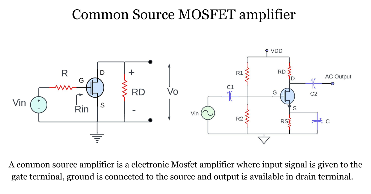
Definition of Common Source MOSFET amplifier
A common source amplifier is a electronic Mosfet amplifier where input signal is given to the gate terminal, ground is connected to the source and output is available in drain terminal.
What is Common Source MOSFET amplifier
A common- source MOSFET amplifier is an electronic amplifier circuit that specifically designed for providing very high Input impedance, in this CS configuration the input signal is given to the gate terminal of transistor while the output is taken at drain terminal. at the same time source terminal is connected to the ground that’s why this amplifier is called as common–source amplifier. This are commonly used for audio amplification and such other electronic due to its ability to provide gain and voltage amplification.
Working principle of common source MOSFET amplifier
As we have already discussed in our previous tutorials in in The Best Study Of MOSFET Amplifiers -Types And Applications so in this tutorial, we will learn how the MOSFET can be used as an amplifier in the common source configuration. And using the small-signal analysis, we will also find the expression of the voltage gain, the input impedance, and the output impedance of the amplifier.
when the MOSFET is used as an amplifier, then typically, it can be used in three configurations. That are
Common source Mosfet amplifier (CS)
Common drain Mosfet amplifier (CD)
Common gate Mosfet amplifier (CG)
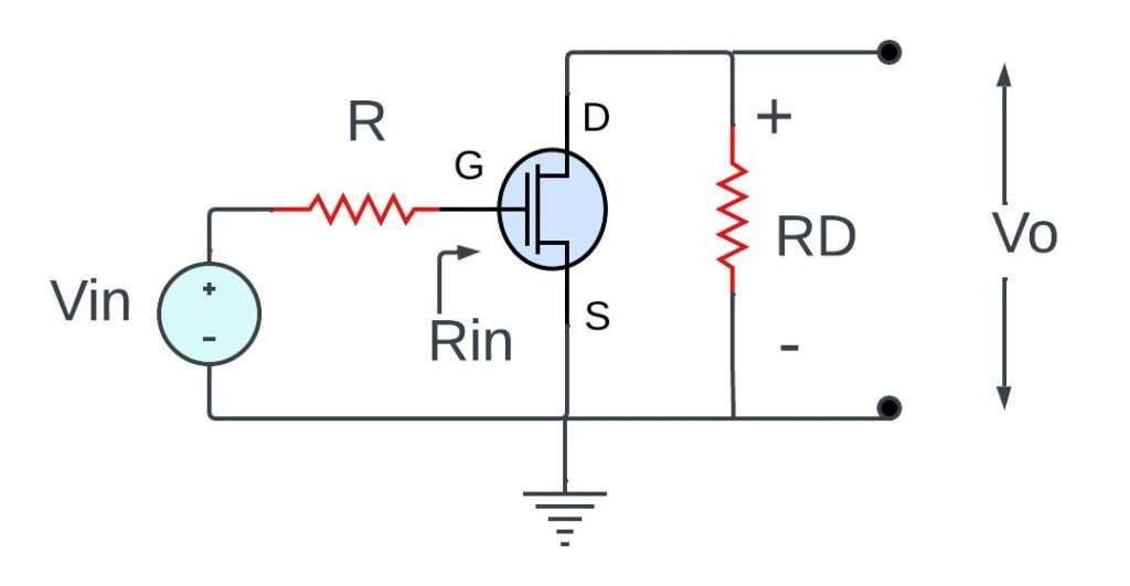
The common source is by far the most popular MOS amplifier configuration. So, in this configuration, the small input signal is applied between the gate and the source terminal. While the output is measured between the drain and the source terminal.
So, that means as far as the AC signal is applied at input then the source terminal is common between the input and the output side (via ground) And hence, this configuration is known as the common source configuration. Now, for any voltage amplifier some of the important parameters are the voltage gain, the input and output impedance etc.
By using the small-signal analysis, it is possible to find all these parameters. As we have Known MOSFET can be replaced by the small-signal model. So. And using this model, it is possible to perform small-signal analysis of the amplifier circuit.
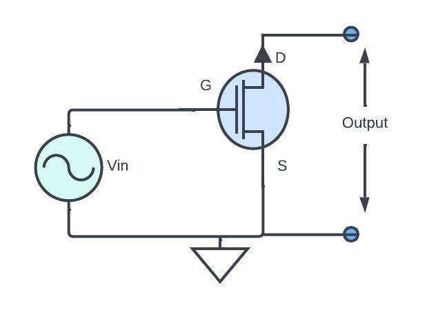
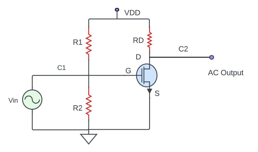
But practically, this is how the MOSFET is look like. here using the coupling capacitors (CC), the input signal is coupled to the amplifier. So, for the DC analysis, all these capacitors will act as an open circuit. And as we can see, hear the MOSFET is biased in the voltage divider biasing configuration. So, from using the DC analysis, it is possible to set the operating point.
Operation of Common Source MOSFET amplifier
A small input signal is applied through the coupling capacitors. So, for AC analysis, or for small-signal analysis, all the DC voltage sources in the circuit will act as a zero. While at the operating frequency, the coupling and the bypass capacitors, will provide very low resistance.
for simplicity, they can be replaced by the short circuit. And then after, the MOSFET will get replaced by the small-signal model. In any circuit for performing AC analysis we need to follow three steps.
- Firstly, replace all the coupling and the bypass capacitors by the short circuit.
- Then consider all the DC sources in the circuit as zero.
- Replace the MOSFET by the small-signal model.
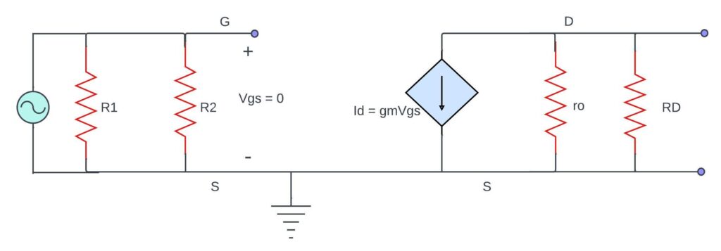
So, here since the bypass capacitor acts as a short circuit, so resistor Rs will also get short-circuited. the input signal is appearing between the between the gate and the source terminal. The resistors R1 and R2 is connected between gate and ground terminal. Similarly, the Rd resistor will appear between the drain and the source terminal. if we see the small-signal equivalent circuit, then it will look like this.
Common Source Mosfet Amplifier key formulas
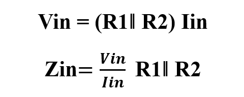
input impedance:

Here; Vin input signal
Iin is the input current
at the low frequencies, the input impedance of the MOSFET is very high. Or it can be infinite. So, for achieving the high input impedance, the value of resistor R1 and R2 should be very high.
output impedance:
now let us find the output impedance- output impedance is Thevenin’s equivalent impedance which can see from the output side. And to find that, we must consider all the input signal as zero Now, since the resistor R1 and R2 are connected in parallel with the input signal, so they will also get short-circuited.
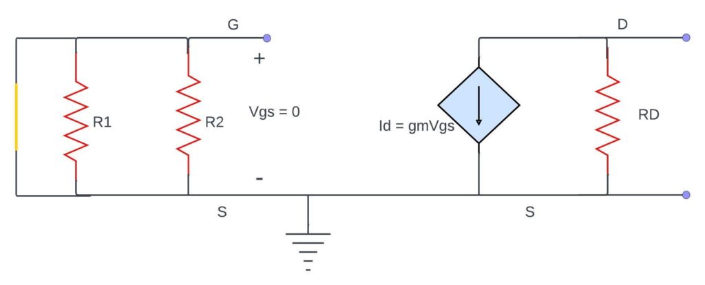
And once the Vin is zero, then voltage Vgs is become zero. Because the voltage between the gate and the source is equal to the input signal. That means the dependent current source, will also act as a zero. Or we can say that it will act as an open circuit. So, in this case, the Thevenin’s equivalent impedance is equal to Rd. Or we can say that the output impedance is equal to Rd.
Zo = Rd
voltage gain:
now let’s find the voltage gain the output is measured between the drain and the source terminal. And since this drain current Id is flowing in this anti-clockwise direction, so we can say that
Vo = -IdRd = -gmVgsRd
And as we know, this voltage Vgs is equal to Vin. So, from this, we can say that,
Vo = -IdRd = -gmVgsRd = -gmVinRd
Vo = -IdRd = -gmVgsRd = -gmVinRd
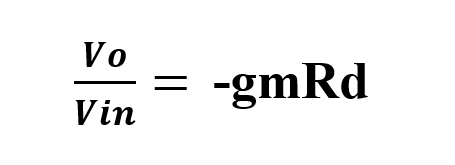
That means the voltage gain is
from this expression, we can say that, by increasing the value of resistor Rd, we can increase the gain. But the value of Rd cannot be increased indefinitely.
This is the small-signal equivalent circuit. So, as you can see, there is an additional output resistance between the drain and the source terminal.
So, in this case, the input impedance will remain the same.
That means in this case,
Zin = R1||R2
the output impedance is equal to Ro || Rd
the voltage gain
Av = -gm*(Rd || Ro)
So, considering the finite output resistance of the MOSFET, these are the expressions of the output impedance, and the voltage gain of this amplifier. this amplifier is biased using this voltage divider biasing configuration
in voltage divider biasing configuration, the source resistor provides negative feedback, and it improves the biasing stability, but whenever, the bypass capacitor is used, then for the AC signal, it will act as a short circuit.
small-signal analysis of common source amplifier
The procedure for the small-signal analysis will remain the same. So,
- firstly, we will replace all the coupling capacitors by the short circuit
- and all the DC sources in the circuit will act as a zero.
- And then after, we will replace the MOSFET by the small-signal model.
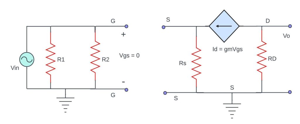
So, the first thing observe is, the source resistor is connected between the source and the ground terminal. And here the input signal is appearing between the gate and the ground terminal.
Similarly, two resistors R1 and R2 are appearing between the gate and the ground terminal. And this resistor Rd is appearing between the drain and the ground terminal. So, if we see the equivalent circuit, then the small-signal equivalent circuit will look like this.
So, for this circuit, first of all, let us find the
voltage gain
Now, here the output voltage
Vo = -id*Rd = -gm*vgs*Rd
So, now, let’s find the relationship between the voltage vgs and the input signal. So, from observation, this drain current Id is also flowing through resistor Rs. That means this voltage
Vs = id*Rs = gm*Vgs*Rs
And here, the voltage between the gate and the ground terminal is equal to Vin. So, if we apply the KVL then we can say that this input signal
Vin = Vgs +Vs = vgs + gm*vgs*Rs = vgs*(1 +gm*Rs)
Or from this, we can say that the voltage
vgs = Vin / (1 + gm*Rs)
So, in this way, we found the relationship between the voltage vgs and the input signal.
input impedance
let’s find the input impedance. So, in this case, the input impedance will remain the same. Because, the gate to source terminal acts as an open circuit. That means the input current Iin is flowing through the parallel combination of the R1 and R2. That mean
Vin = Iin * (R1 || R2)
Or
Vin / Iin, or Zin = to R1 || R2
this is the input impedance for the common source amplifier including the source resistor.
output impedance
to find the output impedance we have to consider all the independent sources in the circuit as zero. That means this input signal will act as a short circuit. And once we consider this Vin as zero, then these two resistors will also get short-circuited.
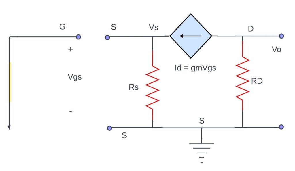
Vgs + Vs = 0
But Vs = Id Rs = gmVgsRs
Vgs + gmVgsRs = 0
Vgs (1+gmRs) = 0
Vgs = 0
And because of that, this voltage the output impedance is since the voltage vgs is equal to zero, so this dependent current source will act as an open circuit.
Zo = Rd
That means in this case also, the output impedance is equal to Rd. So, in this way, we found the expression of the input and the output impedance as well as the voltage gain for this common source amplifier when the source resistor is also present.
Characterises of common source MOSFET amplifier
Here are some Characterises of common source MOSFET amplifier
- Voltage gain: the voltage gain of this amplifier is typically moderate to high And this depends on various factors such as load resistors, biasing and other parameters.
- Input impedance: the Input impedance of CS Mosfet is very high that will make suitable for where the input source has a high impedance.
- Output impedance: when we talk about Output impedance it has moderate impedance and this will impact om load resistance.
- Coupling capacitors: Coupling capacitors are uses for blocking the DC signal and allowing only Ac signal. this signal passes between input to output stages. hence CC is uses for preventing any DC offsets from affecting the output.
- Distortion: in well designed and optimized circuits has less distortion nearly 0.1% to 0.001%. distortion will be affected on linearity
- Noise: Mosfet has generally low noise devices, it depends on various factors such like as temperature, biasing and surrounding condition will affect on overall noise.
- Sensitivity: Sensitivity is the ability of small changes in the input voltage to the output voltage into corresponding changes. It is depending on design, components and uses.
Example
A Mosfet amplifier with a common source is designed with an n-channel MOSFET. It is a thresholds voltage (Vth) is 2.5V and conduction parameter (K) is 50mA/V2. If the supply voltage is +40V and the load resistor (RL) is 600 Ohm.
Find:
1. the value of required resistors to bias the MOSFET amplifier at 1/4 (Vdd). For an undistorted and symmetrical o/p waveform.
2. the DC biasing voltage for drain terminal of the MOSFET to half the supply voltage.
solution:
given values as VDD = +40V, Vth = +2.5V, k = 50mA/V2, RL = 600 Ohm.
- Drain Current (Id)
Vd = Vdd/2 = 40/2 = 20V
Id = Vd/Rd = 10/600 = 16mA
- Gate- source Voltage (Vgs)
Id = k (Vgs-Vth)2
Vgs = √ID/K + Vth = √0.016/0.4 + 2.5 = 2.7V
- Gate voltage (Vg)
Vg = 1/3 Vdd = 40/3 = 13.3
Advantages of common source MOSFET amplifier
- High Voltage Gain: this amplifier provides very high voltage gain that will make it suitable for amplifying weak signals with higher levels without significant distortion.
- High input impedance: the common source configuration has high input impedance that mean they does not draw much current from the preceding stage.
- Good linearity: these MOSFET amplifier can offer good linearity, mean they reproduces the input without making distortion.
- Simplicity: CS amplifier relatively simple in design compared with other configuration. That’s make them suitable for various applications.
Disadvantages of common source MOSFET amplifier
- Limited Bandwidth: this amplifier has limited bandwidth because of capacitance within the circuit. That can reduce their effectiveness in amplifying higher-frequency signals.
- High output capacitance: which can affect there ability to drive capacitive load efficiency, that make issue in stability and reduce performance at higher frequency.
- Temperature Sensitivity: MOSFET are temperature dependent that leads to variation with changes in temperature. It makes challenges while developing the circuits.
- Gain is very high
Applications of common source MOSFET amplifier
- This amplifier is used for signal amplification
- Used in signal processing for filter, equalizer and signal conditioning.
- In other industrial applications for control system and signal in motor drives, automation etc.
Also Read:
The Best Study Of MOSFET Amplifiers
Frequency Asked Questions [FAQs]
Q. Which MOSFET is used for amplifier?
Ans: a common source amplifier uses an n-channel depletion mode MOSFET.
Q. what is common drain Mosfet amplifier?
Ans: the common drain amplifier or source follower uses a Mosfet with input at gate terminal output at source and drain connected to supply voltage.
Q. where is common source amplifier is use?
Ans: they have several applications like- signal processing, RF amplification, ADC circuits etc.
Q. which amplifier is best transistor or Mosfet?
Ans: choosing in between transistor (BJT) and Mosfet it depends on application or uses. BJT has simplicity but low input impedance. Mosfet has high impedance applications, but they need more complex biasing.
Conclusion
In summary, the common source MOSFET amplifier stand out because of its ability to provide voltage gain, moderate input impedance and varieties of applications. A proper biasing and optimization gives impedance matching and fulfil the requirements.
Follow to the blog ETechSpark.com for more articles on electrical engineering, electronic and tech updates.
please leave your question in the comment section, give us your valuable feedback.