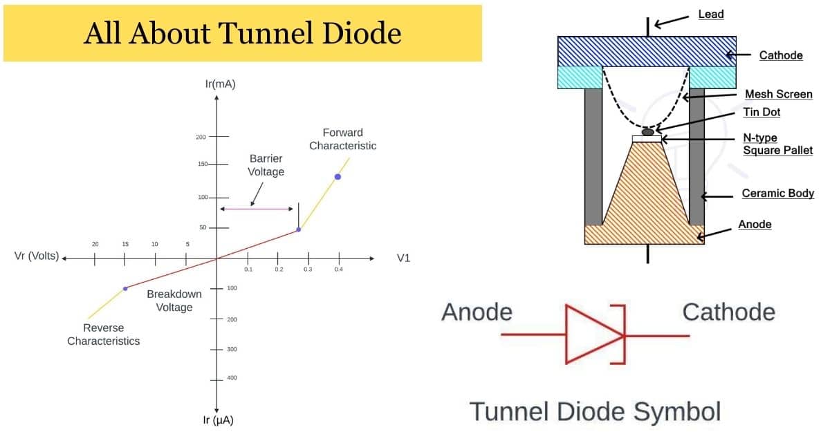
Definition of Tunnel diode
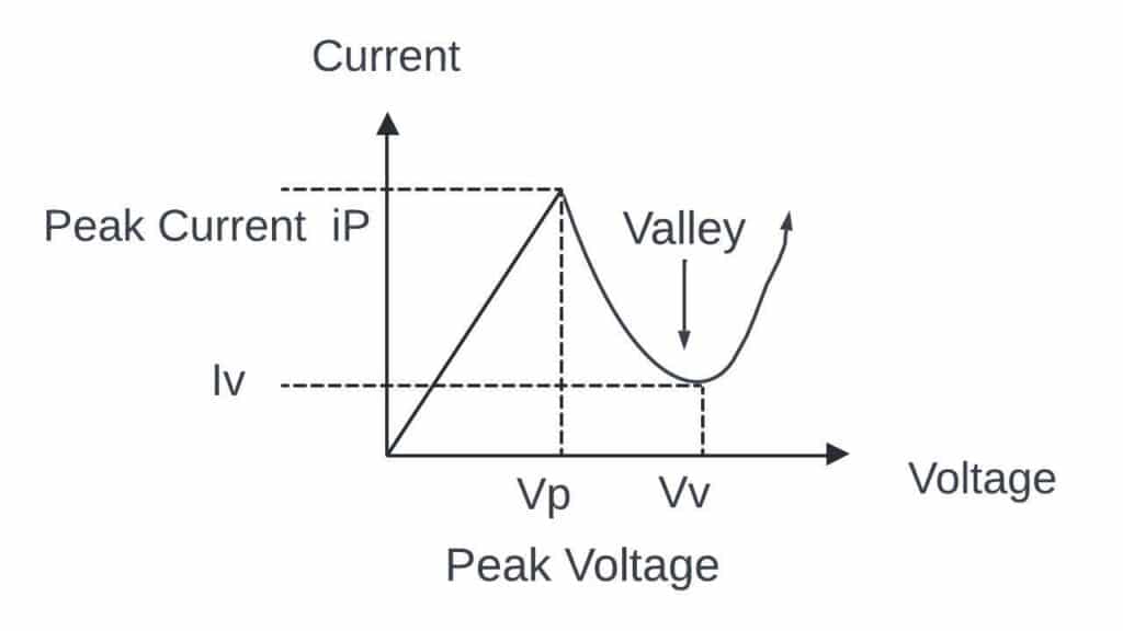
A tunnel diode is a unique semiconductor device that has a distinct current voltage curve. This curve shows that as the voltage increases then the current initially decreases before rising again.
Tunnel diodes are commonly used in high-frequency circuits such as oscillators, amplifiers, and digital systems because they can switch quickly and consume little power.
Tunnel diode symbol
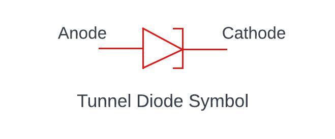
What is a Tunnel Diode?
A tunnel diode, also known as an Esaki diode is a type of semiconductor diode that shows a unique behavior called tunneling effect that allow it to work very fast. It was invented by Leo Esaki in 1957 that is why it sometime called an “Esaki Diode”.
The special thing about a tunnel diode is its negative differential resistance area in the voltage-current curve. This means that as the voltage across the diode goes up then the current goes down before that which have positive differential resistance.
Tunnel diodes are used in high-frequency oscillators, amplifiers, and such as quick switches because they can work really fast. They are great for applications where fast response and low power use are important.
However, they are not as good for low-frequency or low-power uses because of how they work.
Construction of tunnel diode
A tunnel diode is typically constructed using semiconductor materials such as gallium arsenide (GaAs) or silicon (Si) with specific doping to create the desired properties. The basic constructions of a tunnel diode involve several layers those are as follows:
- N-type semiconductor layer:
The diode starts with a heavily doped N-type semiconductor layer which means it has an excess of electrons compared to the intrinsic semiconductor materials.
- P-type Semiconductors layer:
On top of the N-type layer a lightly doped P-type semiconductor layer is deposited. This layer has a deficiency of electrons (Known as “Holes”) compared to the intrinsic semiconductor.

- Metal contacts:
Metal contacts are added to the N-type and P-type layers to allow for external connections.
The key aspect of the Tunnel diode’s construction is the formation of a very thin depletion region between the N-type and P-type layers. This region is created due to the difference in doping concentrations that leading to a high electric field across this junction.
The thinness of the depletion region is crucial for the tunnelling effect to occur. When a voltage is applied across the diode in the Forword bias direction (positive voltage applied to the P-type side and negative voltage to the N-type side).
electrons in the N-type region gain energy and can tunnel through the narrow depletion region into the p-type region. This tunneling phenomenon is what gives the tunnel diode its unique characteristics that including its negative differential resistance behavior.
Working Principle of tunnel diode
The working principle of a tunnel diode is grounded in the fascinating phenomenon of quantum tunneling. When a voltage is applied across a tunnel diode it creates a thin depletion region within the semiconductor material. This region acts as a potential barrier that electrons would traditionally struggle to cross due to their energy levels.
However, in quantum mechanics an electron can exhibits a peculiar behavior known as tunneling. Despite lacking the classic energy required to overcome the barrier and some electrons can tunnel through it.
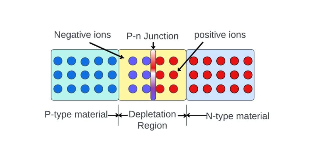
This is possible because of the wave-like nature of electrons that allowing them to pass through regions of space that would be forbidden according to classical physics.
As the applied voltage increases then more electrons tunnel through the barrier that leading to an initial rise in current.
This negative resistance region is a key characteristics of tunnel diodes and finds applications in microwaves oscillators, low-noise amplifiers, and high-speed switching circuits.
Characterises of tunnel diode
Here are the characteristics of a tunnel diodes explained in simpler manner:
- Negative resistance:
Tunnel diodes act differently from most devices. When you increase the voltage then the current goes down and which is opposite to what usually happens.
- Peak current and peak voltage:
There are specific points in the diode’s behavior where it shows maximum negative resistance. These points are called te peak current and peak voltage at these points, the current sharply drops.
- Fast switching:
Tunnel diodes can switch on and off very quickly. This makes them great for things that need to work fast, like microwave circuits.
- Low noise:
They don’t create a lot of electrical noise, which is good for sensitivity electronics that need to stay quiet.
- High-frequency use:
Because they work so quickly tunnel diodes are often used in devices that operates at high frequencies like in radio communications.
- Low power use:
Tunnel diodes don’t need a lot of power to work so they are energy-efficient in electronic systems.
Volt-Amp characteristic
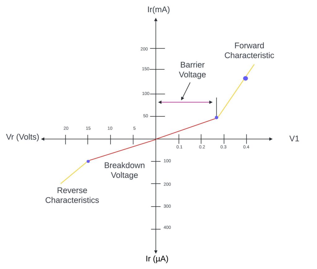
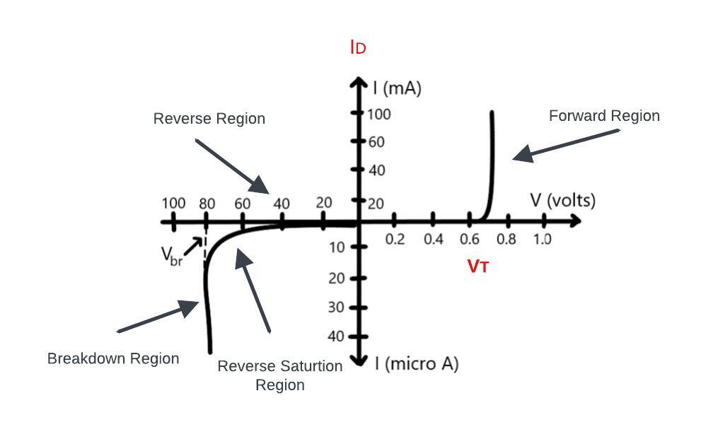
The volt-ampere (V-I) characteristic of a PN junction diode describes how the current passing through the diode changes with the applied voltage in unbiased, reverse biased and forward biased conditions.
1. Unbiased (Zero Bias):
In unbiased conditions no external voltage is applied across the diode. This results in a natural potential barrier at the junction. Caused by the difference in doping levels between the P-type and N-type semiconductors.
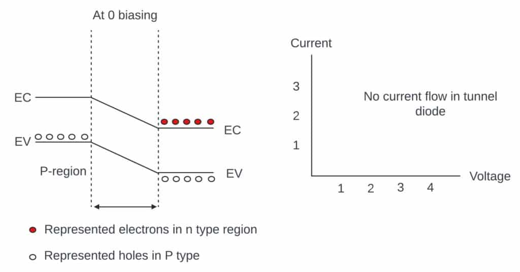
Due to this barrier, there is minimal current flow through the diode.
2. Reverse bias:
In reverse bias the positive terminal of the voltage source is connected to the N-type semiconductor and the negative terminal is connected to the P-type semiconductors.
This creates a barrier that prevents significant current flow. The main carriers (electrons in N-type and holes in P-types) are paused away from the junction.
A small reverse saturation current IRS this flows due to other carriers (those that cross the junction due to thermal energy).
The V-I characteristics in reverse bias is almost a flat line until the breakdown voltage is reached so beyond which the current sharply increases due to breakdown.
3. Forward bias:
In forward bias the positive terminal of the voltage source is connected to the P-type semiconductors and the negative terminals is connected to the N-type semiconductors.
This reduces the barrier at the junction so allowing main carrier to easily cross the junction.

The current increases exponentially with increasing voltage that following a specific equation.
The forward voltage drop across the diode has typically around 0.7 Volts for silicon diodes is relatively constant until the current increases significantly.
Width of the depletion region in tunnel diode
The depletion region’s width in tunnel diode is usually extremely small nearly around a few nanometers or even less. This is because tunnel diodes have a heavily doped P-N junction that making the depletion region narrow compared to other diodes.
This narrow region enables quantum tunneling of electrons which is crucial for tunnel diode’s distinctive properties like negative differential resistance.
Other Types of tunnel diode
- Single-well tunnel diode
This type has a single potential barrier that electrons can tunnel through. It’s often used in low-power applications and a basic building block in electronic circuits due to its simplicity.
- Double-barrier tunnel diode
Featuring two potential barrier this diode offers enhanced tunneling characteristics compared to the single-well type. It’s used in applications requiring precise control of tunneling currents such as in quantum computing devices.
- Superlattice tunnel diode
This diode employes a superlattice structure which consists of alternating layers of direct semiconductor material. This design allows for fine-tuning of tunneling properties that making it suitable for high-frequency and low-noise applications such as in radio frequency (RF) circuits.
- Resonant tunnel diode
This diode utilizes the quantum mechanical phenomenon of resonant tunneling, where electrons pass through potential barrier at specific energy levels. It’s commonly used in microwave oscillators and amplifiers due to its ability to generate high-frequency signals efficiently.
Applications of tunnel diode
- High-frequency oscillators:
Tunnel diode are used in the construction of high-frequency oscillators due to their ability to generate stable oscillations at microwave frequencies.
- Amplifier:
They are utilized as amplifier in microwave circuits for essentially in low-noise amplifier and fast switching circuits.
- Mixture and converters:
Tunnel diodes are employed in mixers and converters to combined or convert signals in radio frequency and microwave systems.
- Pulse generators:
Their fast-switching speed makes tunnel diodes suitable for pulse generation in radar systems, pulse-width modulation (PWM) circuits and digital systems.
- Detector and demodulator circuits:
Tunnel diodes are used as detectors and demodulators in communication systems for detecting and extracting information from modulated signals.
- Logical circuits:
They are used in logical circuits particularly in ultra-high speed digital circuits where their fast switching characterises are advantages.
- Temperature sensors:
This diode exhibits a unique negative temperature coefficient of resistance ((NTC) that making them suitable for temperature sensing applications.
- Voltage-controlled oscillators (VCOs):
Tunnel diode can be incorporated into VCOs for generating frequency-modulated signals in applications such as frequency synthesizer and phase-locked loops (PLLs).
Explain Tunnel diode oscillator
A tunnel diode oscillator is a device that uses a special type of diode to make fast vibrations. This diode can quickly switch between low and high energy states with very little voltage change.
In the oscillator the diode is set up to switch back and forth rapidly that kind of like a mini energy roller coaster. This switching along with some other electronic tricks so it helps create a steady humming sound at a specific frequency.
These types of oscillators are used in things like cell phones, Wi-Fi routers and radar systems because they can make signals that travel fast and stay stable.
Advantages and disadvantages of tunnel diode
Advantages
High speed operation
Low noise
Low power consumption
Temperature stability
Compact size
Disadvantages
Limited voltage range
Temperature sensitivity
Limited applications
Limited market availably
Frequently asked questions
Q. What is the difference between normal diode and tunnel diode?
Ans: the main difference between a normal diode and a tunnel diode lies in their voltage-current characteristics. A normal diode operates based on the principle of forward and reverse bias that allowing current flow in forward bias and blocking it in reverse bias.
On the other hand, a tunnel diode exhibits a negative resistance region in its voltage-current characteristics curve that meaning its current decreases as voltage increases within a specific voltage range.
Q. What is the difference between Zener diode and tunnel diode?
| Feature | Zener Diode | Tunnel Diode |
|---|---|---|
| How it works | Allows current when voltage is high enough | Current decreases with increasing voltage in a certain range |
| Voltage-current | Has a steady breakdown voltage | Shows negative resistance in its behavior |
| Characteristics | Keep voltage stable during breakdown | Current decreases as voltage rise |
| Use | Voltage regulation, protection against too much voltage | High-frequency circuits like fast-switching and amplification |
Q. What is tunnel diode size?
Ans: tunnel diode is usually very small are measured in micrometer (µm) or nanometer (nm) near 10 nm due to their design for high-frequency and low power applications.
Q. Is Gunn diode a tunnel diode?
No, a Gunn diode is not a tunnel diode. They are different types of diodes with distinct operating principles and characteristics.
While both diodes are used in electronic circuits a Gunn diode operates based on the Gunn effect, which involves the formation of electron domains in certain semiconductor materials like gallium arsenide (GaAs).
In contrast a tunnel diode operates based on quantum tunneling phenomena across a narrow barrier in its structure.
Q. Which semiconductor is used in tunnel diode?
Ans: the semiconductor typically used in tunnel diodes is heavily doped germanium or gallium arsenide (GaAs).
Q. Are diode AC or DC?
Ans: diodes can conduct both AC (Alternating Current) and DC (Direct Current) depending on their configuration and the applied voltage.
Explanation–
In a forward-biased condition diodes allow current to flow in one direction that makes them conductive for both AC and DC. However, in reverse bias diodes block current flow to making them non-conductive for both AC and DC.
Conclusion:
Tunnel diodes, known for their special resistance behavior, work well in fast and quiet applications like microwave oscillators. Although they have limits like being sensitive to temperature and needing specific voltages and learning about them helps use them better in electronic design.
Also Read:
Diode Definition, Types of Diodes, V-I Characteristics & Application
How Freewheeling Diode Work: Easy Explanation
VI Characteristics Of Pn Junction Diode- Comprehensive Study
